Display device

a technology display devices, which is applied in the field of display devices, can solve the problems of lowering the likelihood of threshold values and affecting the operation stability, and achieve the effect of enhancing the time-wise likelihood of a leak current of floating memory nodes

Active Publication Date: 2009-09-10
PANASONIC LIQUID CRYSTAL DISPLAY CO LTD +1
View PDF9 Cites 4 Cited by
  • Summary
  • Abstract
  • Description
  • Claims
  • Application Information

AI Technical Summary

Benefits of technology

[0037]To briefly explain advantageous effects acquired by the typical inventions among the inventions described in this specification, they are as follows.
[0038]According to the present invention, in the display device having a single-channel shift register circuit, the number of times of writing of a voltage in the floating memory node can be increased thus enhancing time-wise likelihood for a leak current of the floating memory node.

Problems solved by technology

Accordingly, leak currents from the floating memory nodes influence the operational stability.
. . in FIG. 9) are increased and hence, a stable operation is deteriorated resulting in a possibility of lowering of likelihood of the threshold values.

Method used


Image

  • Display device
  • Display device
  • Display device

Examples


embodiment 1

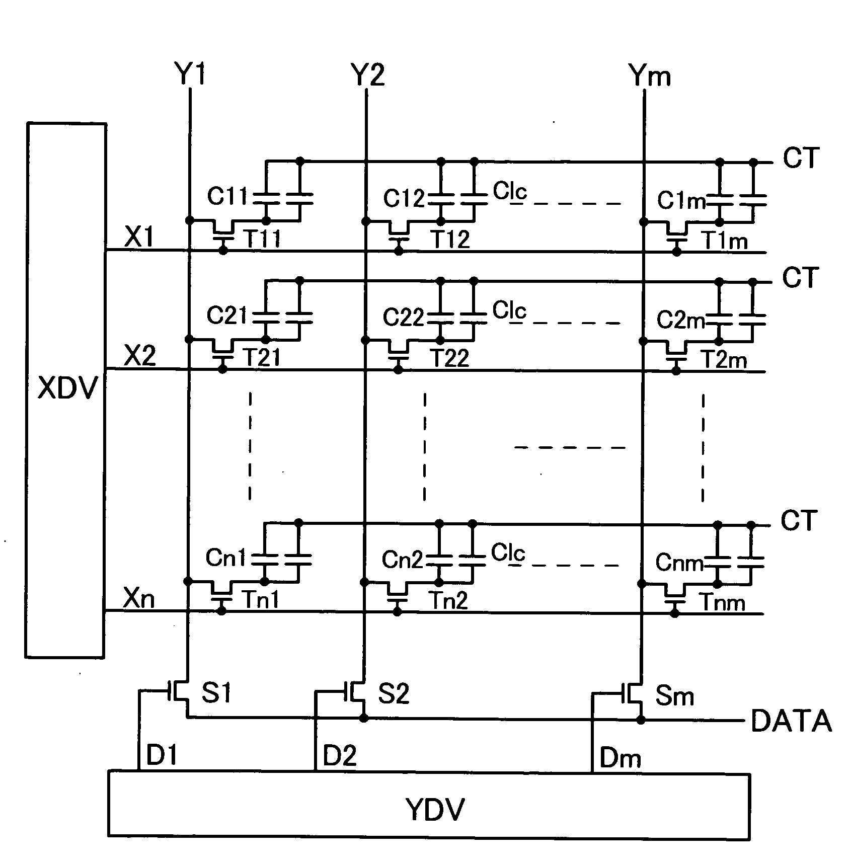
[0050]FIG. 1 is a circuit diagram showing an equivalent circuit of a liquid crystal display panel of an active-matrix-type liquid crystal display device of an embodiment 1 according to the present invention.

[0051]As shown in FIG. 1, the liquid crystal display panel of this embodiment includes, on a liquid-crystal-side surface of one substrate out of a pair of substrates which is arranged to face each other in an opposed manner with liquid crystal therebetween, n pieces of scanning lines (also referred to as gate lines) (X1, X2, . . . Xn) which are arranged parallel to each other in the y direction and extend in the x direction and m pieces of video lines (also referred to as source lines or drain lines) (Y1, Y2, . . . Ym) which are arranged parallel to each other in the x direction and extend in the y direction.

[0052]Regions which are surrounded by the scanning lines and the video lines constitute pixel regions. Each pixel region is provided with an active element (thin film transis...

embodiment 2

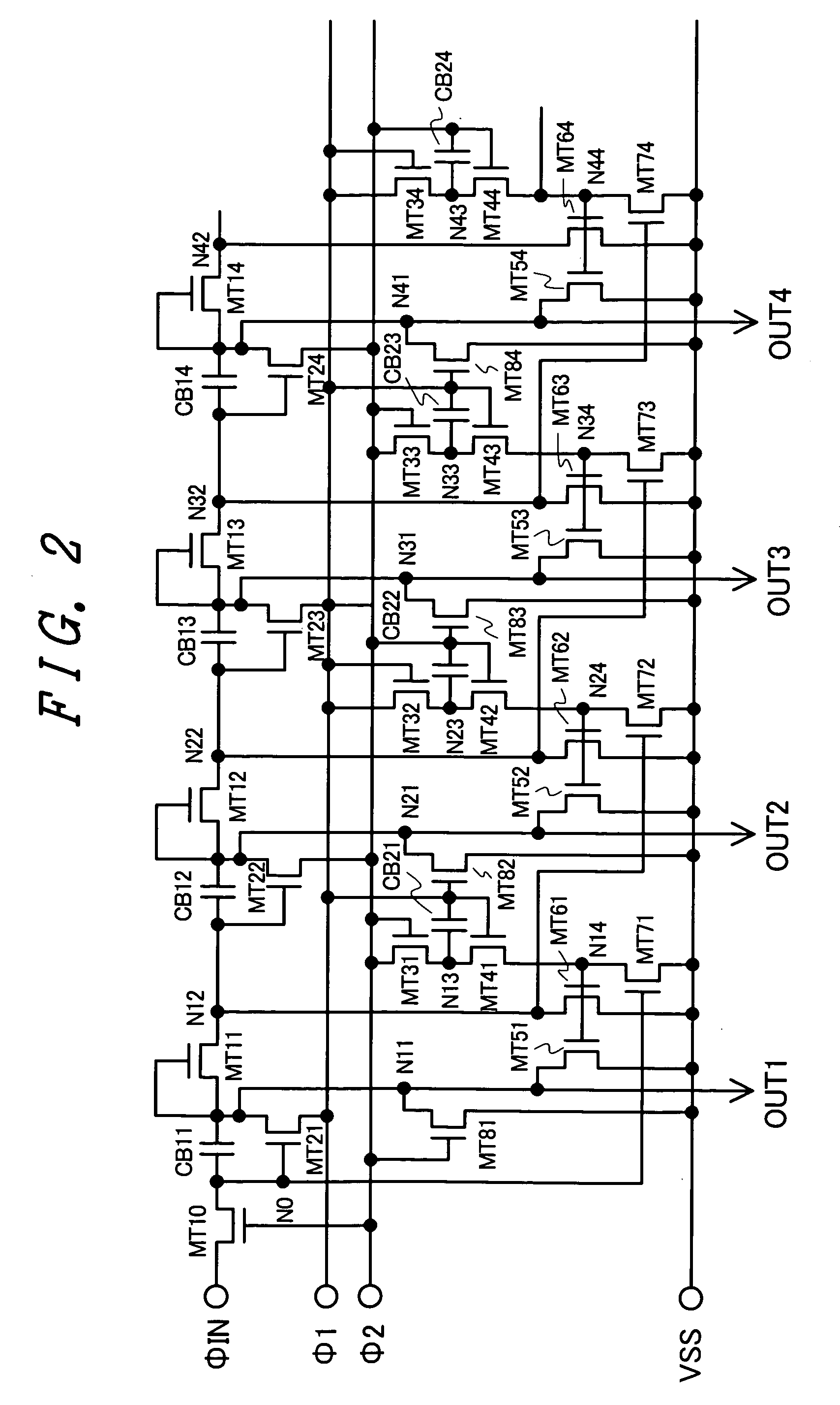
[0107]FIG. 5 is a circuit diagram showing the circuit constitution of a shift register circuit of an embodiment 2 according to the present invention.

[0108]This embodiment is characterized in that, in the circuit shown in FIG. 2, the transistors (MT5*, MT6*, MT7*) which are exclusively used for resetting are formed of a transistor having the double gate structure thus realizing the enlargement of likelihood of a leak current.

embodiment 3

[0109]FIG. 6 is a circuit diagram showing the circuit constitution of a shift register circuit of an embodiment 3 according to the present invention.

[0110]This embodiment is characterized in that, in the circuit shown in FIG. 5, a transistor (fifth transistor of the present invention) (MT9*) is inserted between the source of the transistor (MT1*) of each basic circuit and the gate of the transistor (MT2*) of the basic circuit of the succeeding stage. Here, a fixed bias voltage (VDD) having an H level is inputted to the gate of the transistor (MT9*).

[0111]The transistor (MT9*) is provided for preventing the further elevation of the voltage of the node (N*2) exceeding approximately the voltage (VDD−Vth) even when the voltage of the node (N*5) is elevated due to the bootstrap effect. As a result of the prevention of further elevation of the voltage of the node (N*2), the elevation of the drain voltage when the transistor (MT5*) is turned off can be suppressed thus enhancing the likelih...


PUM


Abstract

In a display device which includes a driver circuit having a shift register circuit, the shift register circuit is constituted of basic circuits in plural stages. Each basic circuit is constituted of a circuit A, a circuit B and a circuit C. The circuit A fetches a first drive clock (or a second drive clock) inputted from the outside when transfer data is inputted to the circuit A from a circuit of preceding stage, outputs the transfer data as a shift output of own stage, and transfers the transfer data to the circuit B. The circuit B transfers the transfer data to the circuit A of the basic circuit of the succeeding stage, and resets the circuit C. The circuit C resets the circuit A and the circuit B in synchronism with the first drive clock (or the second drive clock) generated at next timing or succeeding timing of the first drive clock.

Description

[0001]The present application claims priority from Japanese applications JP2008-053314 filed on Mar. 4, 2008, the content of which is hereby incorporated by reference into this application.BACKGROUND OF THE INVENTION[0002]1. Field of the Invention[0003]The present invention relates to a display device, and more particularly to a technique which is effectively applicable to a display device having a shift register circuit.[0004]2. Description of the Related Art[0005]For example, in an active-matrix-type liquid crystal display device which uses thin film transistors (TFT) as active elements, on a liquid-crystal-side surface of one substrate out of substrates which are arranged to face each other in an opposed manner with liquid crystal sandwiched therebetween, pixel regions are formed. Each pixel region is surrounded by two scanning lines which extend in the x direction and are arranged parallel to each other in the y direction and two video lines which extend in the y direction and a...

Claims


Application Information

Patent Timeline
Patent Type & Authority Applications(United States)
IPC IPC(8): G09G3/36
CPCG09G3/3677G11C19/184G09G2310/0286G09G3/3688
Inventor MIYAZAWA, TOSHIOMAKI, MASAHIROSATO, HIDEOSHIGAKI, TAKUMI
Owner PANASONIC LIQUID CRYSTAL DISPLAY CO LTD
Why Eureka
Try Eureka