

Plasma Display Device
a display device and plasma technology, applied in the field of plasma display devices, can solve the problems of increasing power consumption, insufficient conduction resistance of output elements, and small operation margin of plasma display panels, so as to secure the operation margin of plasma displays, reduce the resistance of output elements, and reduce the amplitude of drive pulses
- Summary
- Abstract
- Description
- Claims
- Application Information
AI Technical Summary
Benefits of technology
Problems solved by technology
Method used
Image

Examples
first embodiment
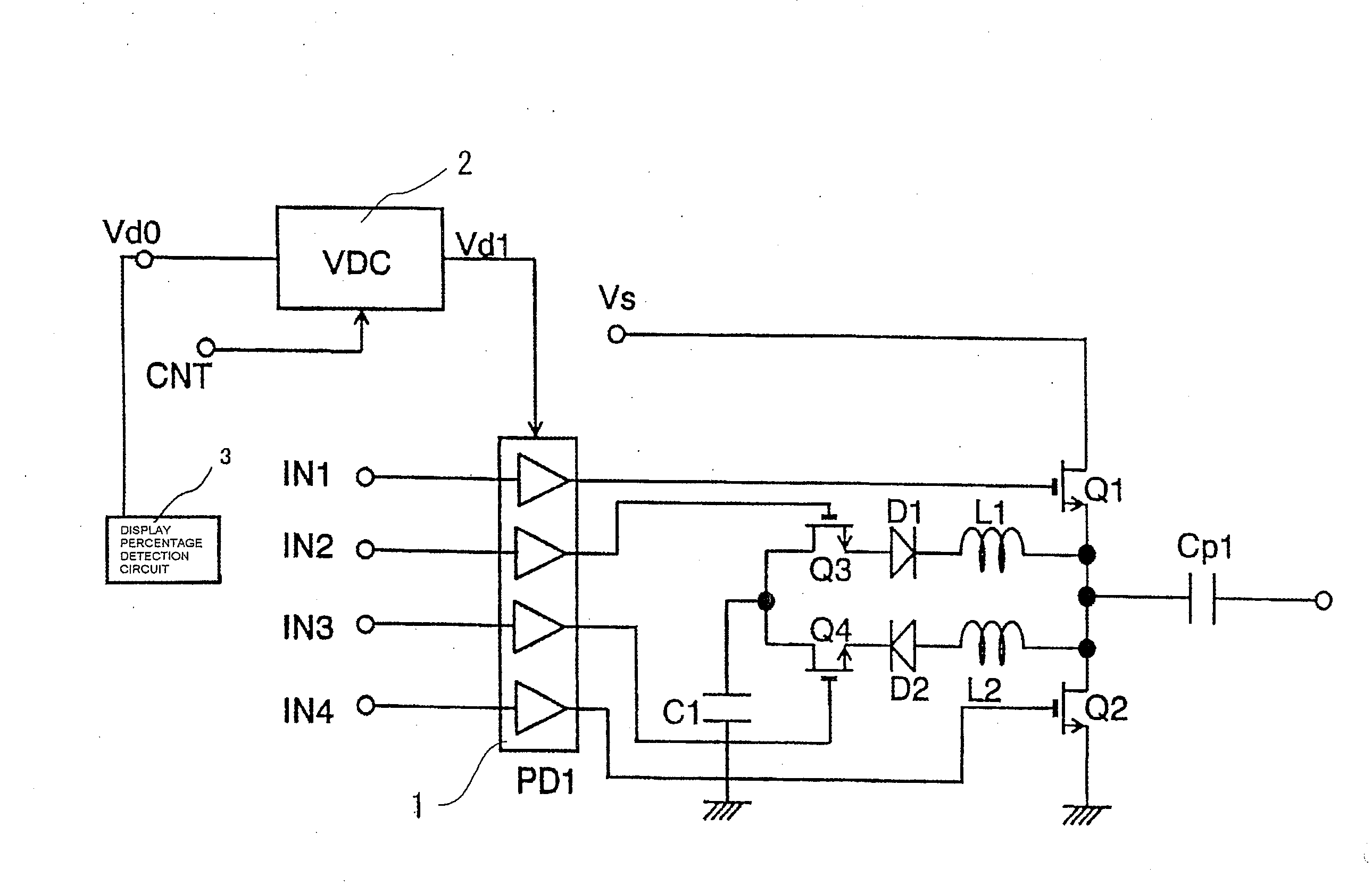
[0033]FIG. 1 shows a first embodiment of a sustain circuit of a plasma display device according to the present invention including a plasma display panel shown in FIG. 6 for instance.
[0034]In FIG. 1, reference character PD1 denotes a pre-drive circuit which forms a drive pulse for driving output elements of a sustain circuit. PD1 forms the drive pulse for driving output elements Q1 to Q4 based on inputted signals IN1 to IN4.
[0035]Reference character VDC2 of FIG. 1 denotes a drive voltage control circuit, which controls a power supply voltage vd1 of a pre-drive circuit 1 based on a control voltage CNT and is supplied with a display percentage of the plasma display device detected by a display percentage detection circuit 3.
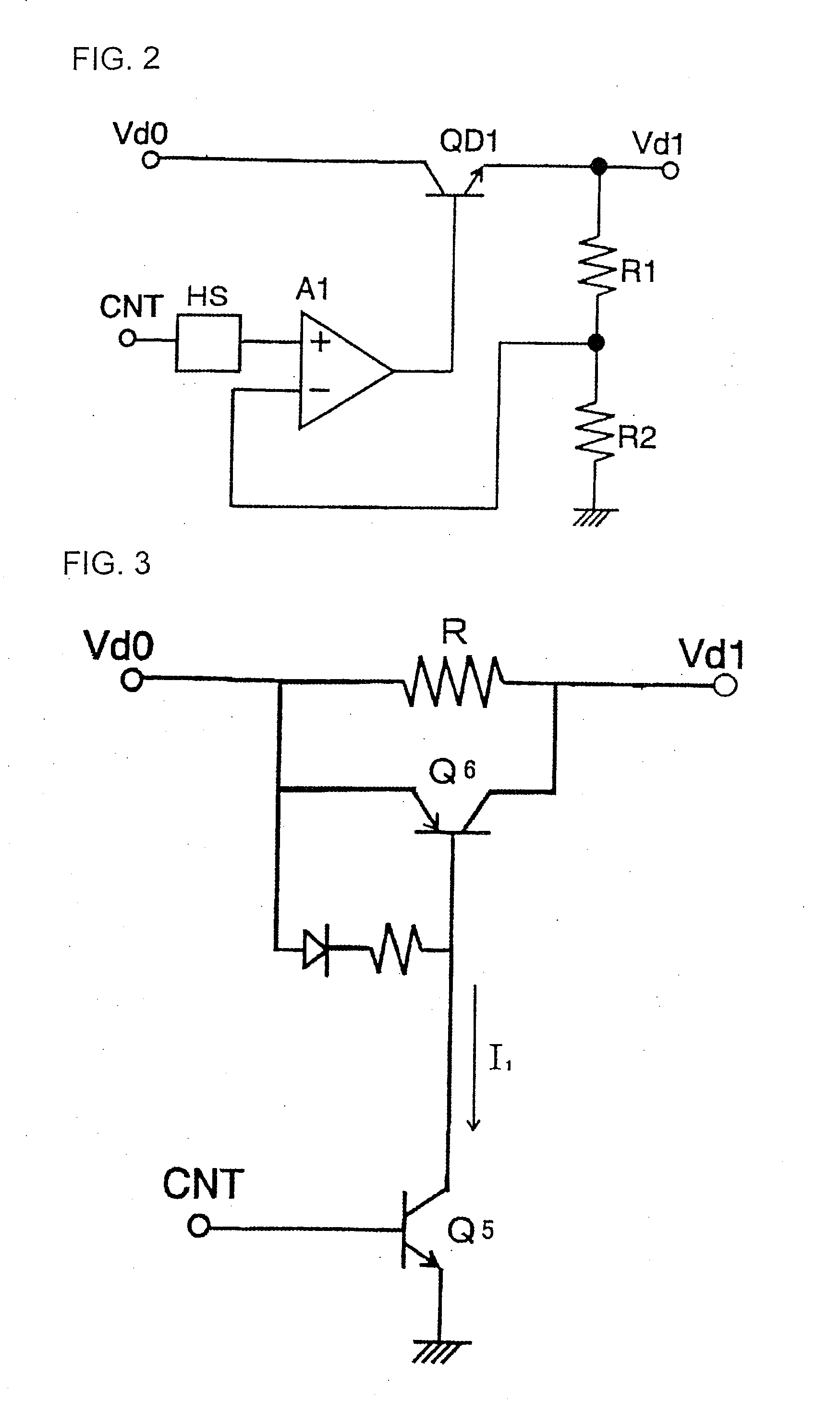
[0036]FIG. 2 shows a concrete example of a drive voltage control circuit 2 described in FIG. 1.
[0037]In FIG. 2, reference character QD1 denotes a transistor, A1 denotes a differential amplifier circuit, and R1 and R2 denote resistances. The resistances R1 and R2 de...
second embodiment
[0050]FIG. 4 shows a second embodiment of the sustain circuit of the plasma display device according to the present invention.
[0051]The sustain circuit of the plasma display device shown in FIG. 4 detects a sustain current passing through the output element Q1 in a resistance R11.
[0052]The drive voltage control circuit VDC2 controls the power supply voltage Vd1 to be supplied to the pre-drive circuit 1 (PD11) according to the voltage detected in the resistance R11.
[0053]The sustain circuit of the plasma display device shown in FIG. 4 heightens Vd1 when the sustain current passing through Q1 is large, and increases the amplitude of the drive pulse to be supplied to Q1. As a result of this, it is possible to reduce the conduction voltage of Q1.
[0054]The display percentage and the size of the sustain current are generally correlated, where the sustain current is large when the display percentage is large.
[0055]Therefore, it is possible, according to the configuration of this embodiment...
third embodiment
[0056]FIG. 5 shows a third embodiment of the sustain circuit of the plasma display device according to the present invention.
[0057]The sustain circuit of the plasma display device shown in FIG. 5 detects a sustain current passing through the output element Q1 in a coil L11.
[0058]The drive voltage control circuit VDC2 controls the power supply voltage Vd1 to be supplied to the pre-drive circuit 1 (PD11) according to the voltage detected in the coil L11.
[0059]The circuit shown in FIG. 5 heightens Vd1 when the sustain current passing through Q1 is large, and increases the amplitude of the drive pulse supplied to Q1. As a result of this, it is possible to reduce the conduction voltage of Q1.
[0060]The display percentage and the size of the sustain circuit are generally correlated, where the sustain circuit is large when the display percentage is large.
[0061]Therefore, it is possible, according to this embodiment as with the first and second embodiments, to secure the operation margin by ...
PUM
 Abstract
Description
Claims
Application Information