Display device

a display device and display technology, applied in the field of display devices, can solve the problems of reducing the effective light emitting time, erroneous light emission, non-uniform in-plane brightness, etc., and achieve the effects of low resistance, reduced chip size of scanning driver, and reduced modulation circui

Inactive Publication Date: 2007-03-08
HITACHI DISPLAYS
View PDF0 Cites 1 Cited by
  • Summary
  • Abstract
  • Description
  • Claims
  • Application Information

AI Technical Summary

Benefits of technology

[0009] The present invention is made by making use of the above-mentioned characteristics of the electron emission element, wherein by setting an ON resistance of a non-selection switch in a scanning circuit larger than an ON resistance of a selection switch in the scanning circuit, an element size of the non-selection switch can be made small thus decreasing a chip size of a scanning driver which is formed of a semiconductor integrated circuit constituting a scanning circuit without adversely influencing the display characteristics.
[0010] Further, according to the present invention, by setting a resistance of an output circuit when a voltage of a modulation circuit is changed from a white level voltage to a black level voltage larger than the resistance of the output circuit when the voltage of the modulation circuit is changed from the black level voltage to the white level voltage, an element size of a circuit for changing a voltage in an output circuit to a black level voltage from a white level voltage can be decreased and hence, a chip size of a data driver which is formed of a semiconductor integrated circuit constituting the modulation circuit can be decreased.
[0011] Further, according to the present invention, in view of the characteristics of a transistor that an ON resistance of a bipolar transistor is smaller than an ON resistance of a MOSFET, by forming the selection switch which requires a low ON resistance using the bipolar transistor, an element size can be decreased and hence, a chip size of the scanning driver can be decreased. Here, when the non-selection switch which may have the high ON resistance is formed of an MOSFET which is used in other portion of the scanning driver in the same manner, the increase of the number of steps can be made extremely small.
[0012] In the same manner, by constituting only the output circuit for changing the voltage to the white-level voltage from the black-level voltage, it is possible to decrease the element size while suppressing the increase of the number of steps to a minimum.
[0013] Further, according to the present invention, by arranging the bipolar transistor which constitutes the output circuit closer to an output than the MOSFET, even when a high voltage is generated on display panel wiring due to an abnormal discharge phenomenon, a junction between a collector diffusion layer and a substrate of the bipolar transistor is made in the forward direction and hence, an electric current flows in the substrate whereby the elevation of the voltage of the MOSFET part is decreased. As a result, there is no possibility that a gate insulation film of the MOSFET is broken.
[0014] According to the present invention, since the chip size of the semiconductor integrated circuit which constitutes the drive circuit can be decreased, it is possible to lower a chip unit cost.

Problems solved by technology

In the display device which uses the cold-cathode electron emission element, due to a capacitance attributed to wiring, there arise drawbacks such as a rounding of an output waveform in a drive circuit, the reduction of an effective light emitting time, an erroneous emission of light, a non-uniform in-plane brightness.
However, as described in paragraphs to of the above-mentioned patent document 1, there arises a drawback that a chip size of a semiconductor integrated circuit which constitutes the drive circuit is increased and hence, a chip cost is pushed up.
Particularly, in the display device which uses an MIM-type electron emission element, an insulation film having a thickness of approximately 10 nm is sandwiched by an upper electrode and a lower electrode and hence, a capacitive value of the wiring is large and hence, the above-mentioned drawback becomes outstanding.

Method used


Image

  • Display device
  • Display device
  • Display device

Examples


embodiment 1

[Embodiment 1]

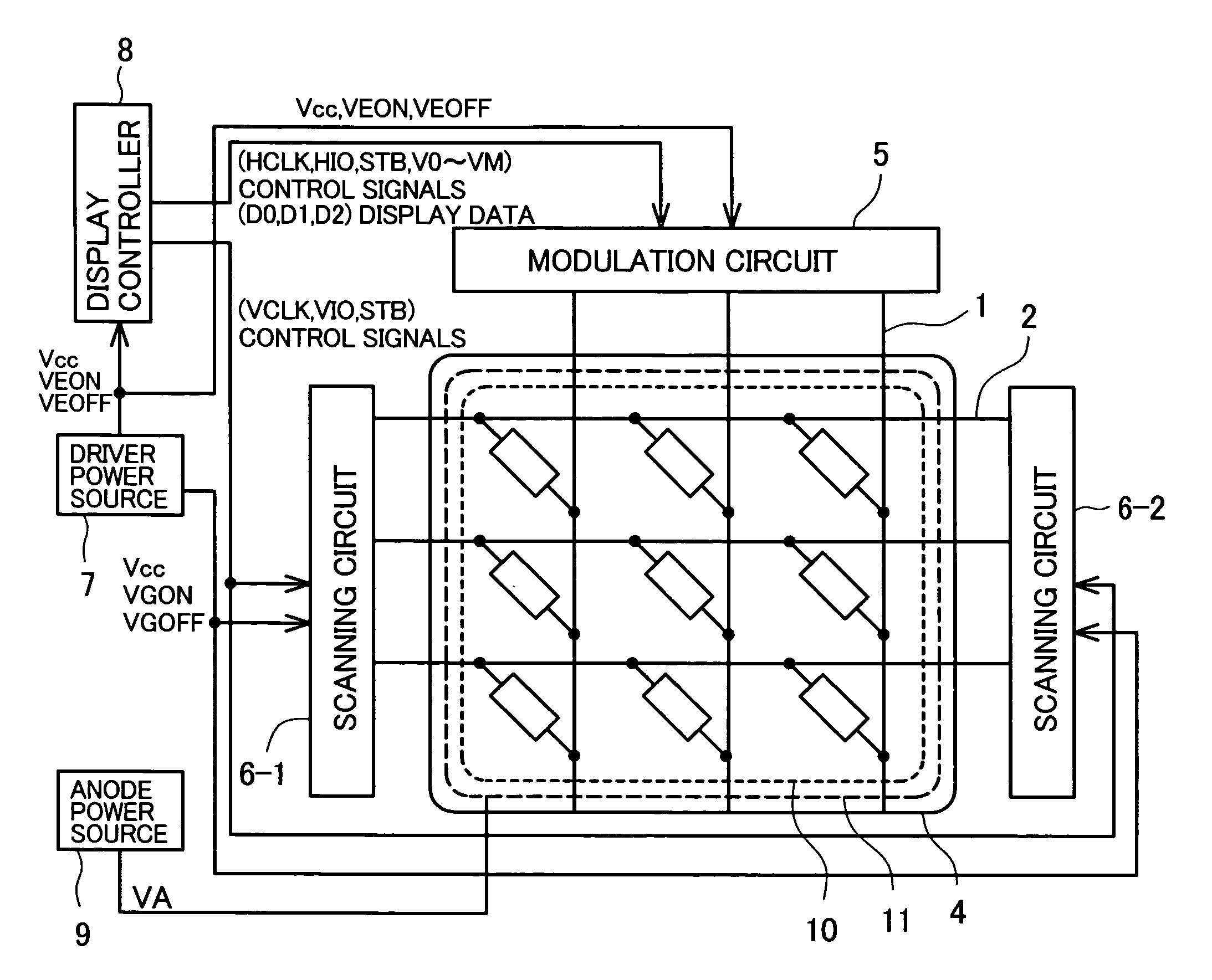
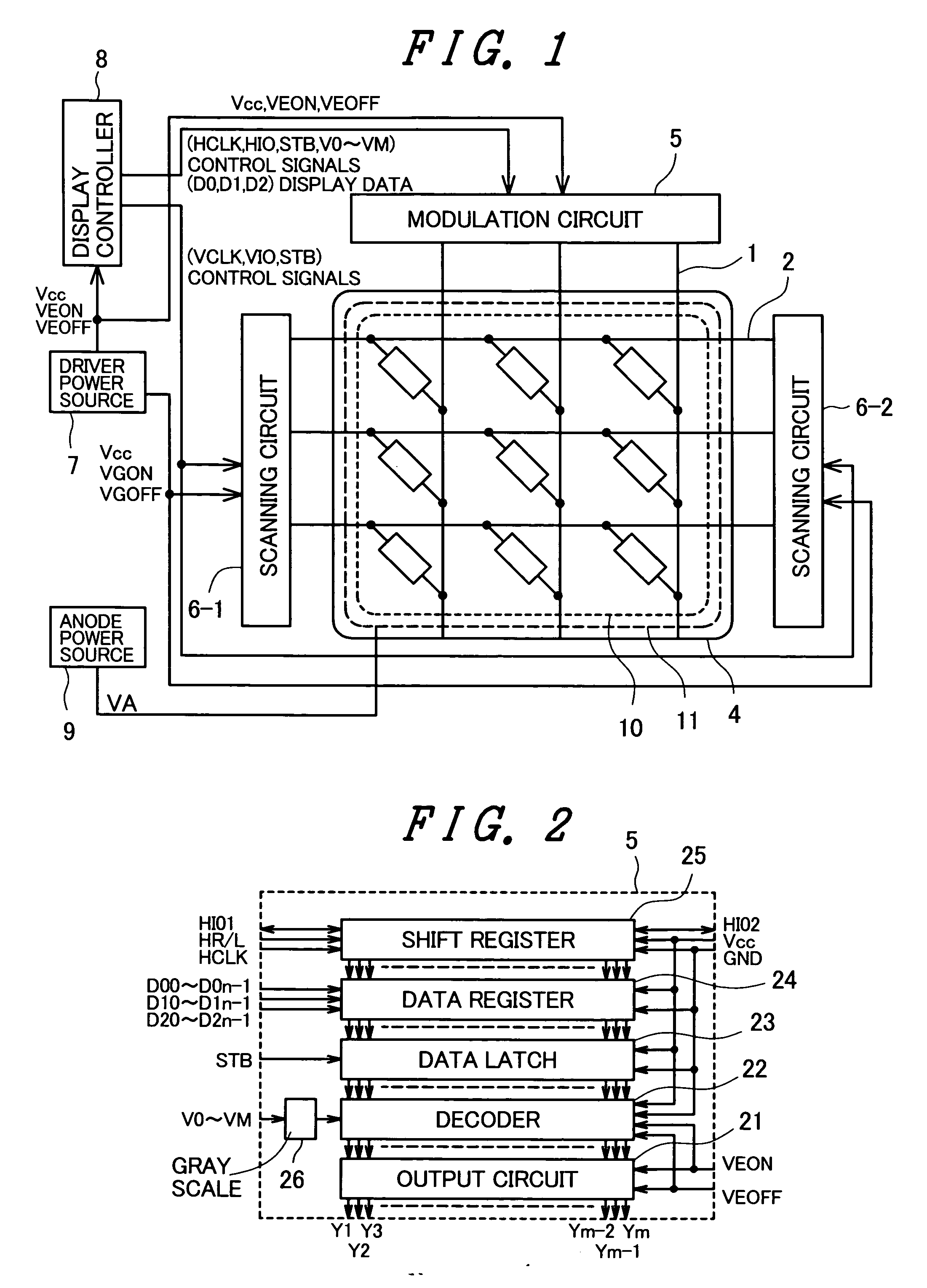
[0033]FIG. 1 is a block diagram showing the whole circuit constitution of a display device which uses MIM-type electron emission elements according to the present invention. On a back plate which constitutes a display panel 4, the MIM-type electron emission elements 3, column lines 1 which are connected with lower electrodes of the MIM-type electron emission elements 3, and row lines 2 which are connected with upper electrodes of the MIM-type electron emission elements 3 are formed. A face plate which constitutes the display panel 4 includes a phosphor film 10, and a metal back 11 which is formed to cover the phosphor film 10 on a surface thereof which faces the back plate. Further, the display panel 4 includes an air discharge port formed in a side wall (not shown in the drawing) which is formed in a periphery of an image display region to evacuate the inside of the panel into a vacuum. The phosphor film 10 is constituted of three primary colors of red, green and blue...

embodiment 2

[Embodiment 2]

[0065] In the above-mentioned embodiment 1, the row line 2 is connected to the upper electrode of the MIM-type electron emission element 3 and the column line 1 is connected to the lower electrode of the MIM-type electron emission element 3. In this embodiment, to the contrary, the column line 1 is connected to the upper electrode of the MIM-type electron emission element 3 and the row line 2 is connected to the lower electrode of the MIM-type electron emission element 3.

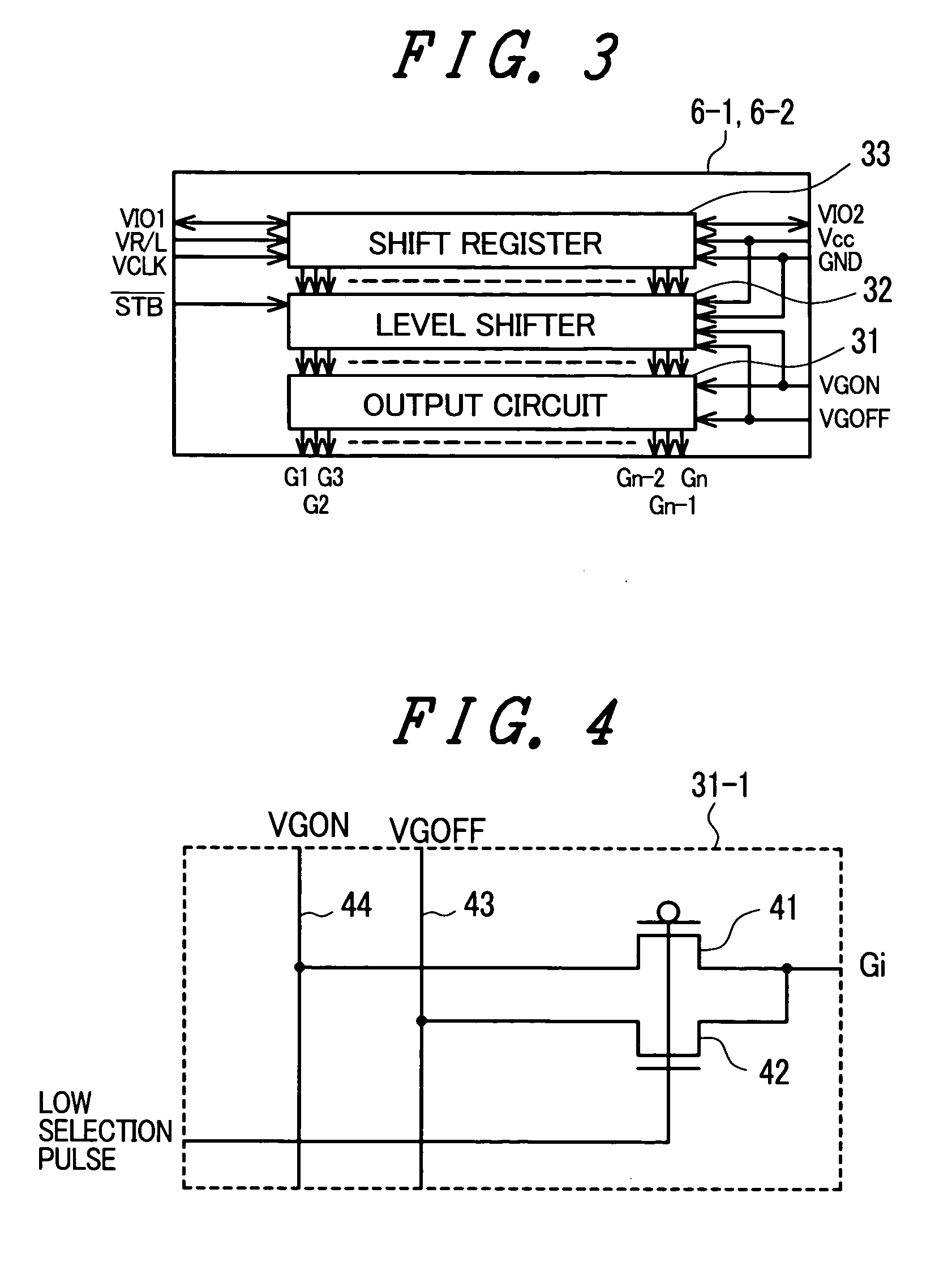
[0066] Due to such a constitution, with respect to the output circuit in the inside of the scanning driver, the pMOS selection switch 41 in the embodiment 1 is used as the pMOS non-selection switch and the non-selection voltage VGOFF is turned on / off by the switch, while the nMOS non-selection switch 42 in the embodiment 1 is used as the nMOS selection switch and the selection voltage VGON is turned on / off by the switch.

[0067]FIG. 7 is a waveform chart of remotest end output voltages of the data driv...

embodiment 3

[Embodiment 3]

[0072]FIG. 8 is a view showing the output circuit 31 in the inside of the scanning driver shown in FIG. 3 in detail. In this embodiment, the PMOS selection switch 41 of the embodiment 1 shown in FIG. 4 is replaced with a pnp transistor 81.

[0073] In FIG. 8, numeral 31-2 indicates a unit of the output circuit 31 which is provided for every line. Numeral 42 indicates an nMOS non-selection switch which turns on / off the non-selection voltage VGOFF, and numeral 81 indicates a pnp transistor selection switch which turns on / off the selection voltage VGON. Further, numeral 43 indicates a power source line which supplies the non-selection voltage VGOFF to the nMOS non-selection switch 42, and numeral 44 indicates a power source line which supplies the selection voltage VGON to the pnp transistor selection switch 81.

[0074] Here, an ON resistance of the nMOS non-selection switch 42 is larger than an ON resistance of the pnp transistor selection switch 81.

[0075]FIG. 9A is a plan...


PUM


Abstract

In a display device which includes a scanning circuit, an ON resistance of a non-selection switch of the scanning circuit is set larger than an ON resistance of a selection switch. By setting the ON resistance of the non-selection switch of the scanning circuit larger than the ON resistance of the selection switch, an element size of the non selection switch can be made small and hence, a chip size of a scanning driver which is formed of a semiconductor integrated circuit constituting a scanning circuit can be made small without adversely influencing the display characteristics of the display device.

Description

BACKGROUND OF THE INVENTION [0001] 1. Field of the Invention [0002] The present invention relates to a display device which uses a cold-cathode electron emission element such as a surface-conductive-type electron emission element, a field-emission-type electron emission element or the like, and more particularly a metal / insulation film / metal (MIM) type electron emission element. [0003] 2. Description of the Related Art [0004] As drive circuits for driving a cold-cathode electron emission element, there have been known a CMOS output buffer which is constituted of a P-channel MOSFET and an N-channel MOSFET (see FIG. 19 of JP-A-2004-86130) (patent document 1) and an output buffer which is constituted of a PNP transistor and an NPN transistor (see FIG. 20 of patent document 1). SUMMARY OF THE INVENTION [0005] In the display device which uses the cold-cathode electron emission element, due to a capacitance attributed to wiring, there arise drawbacks such as a rounding of an output wavefo...

Claims


Application Information

Patent Timeline
Patent Type & Authority Applications(United States)
IPC IPC(8): G09G3/36
CPCG09G3/22G09G2300/06G09G2310/0221G09G2310/0267G09G2320/0233G09G2310/08G09G2320/0209G09G2320/0223G09G2310/0275
Inventor OZAKI, TOSHIFUMITSUKAHARA, MASAHISA
Owner HITACHI DISPLAYS
Why Eureka
Try Eureka