

Slotted damascene lines for low resistive wiring lines for integrated circuit
a technology of integrated circuits and damascene lines, which is applied in the direction of electrical equipment, semiconductor devices, semiconductor/solid-state device details, etc., can solve the problems of global restriction of resistance of metal lines, increased chip size, and strong limit of metal lines
- Summary
- Abstract
- Description
- Claims
- Application Information
AI Technical Summary
Benefits of technology
Problems solved by technology
Method used
Image

Examples
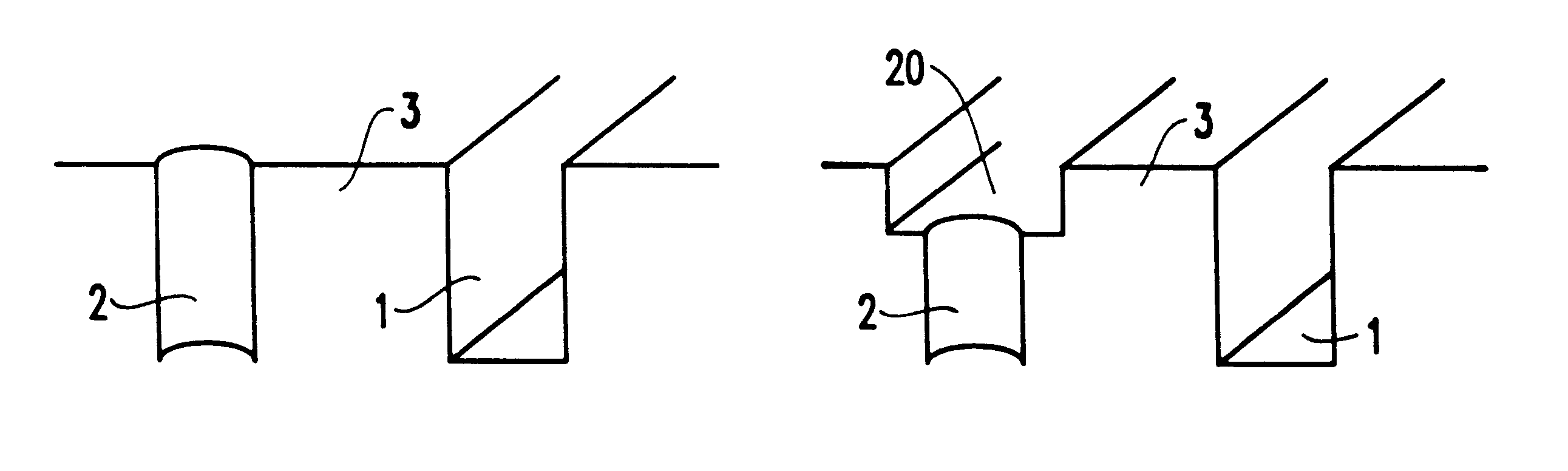
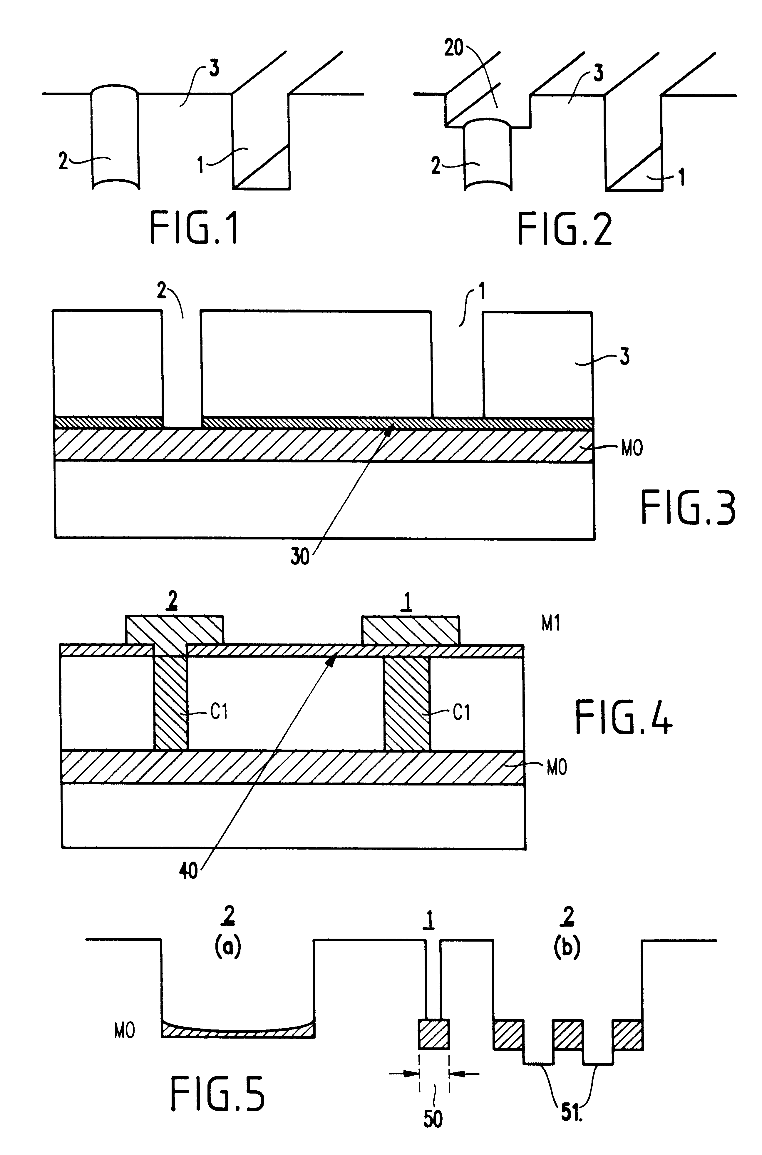
first embodiment
Modifications to the First Embodiment
Several variations of the basic process according to the present invention described above are possible concerning the metal M0 preceding the C1 level and the metal M1 succeeding the C1 level.
For example, in a first modification, in which the slotted lines do not have an underlying M0 metal line and no etch stop layer is introduced, the C1 etch is not self-terminating and must be performed in a time-controlled manner. An advantage to this modification is that the slot can continue even deeper than the M0 level. However, there may be unintentionally long overetching, thereby leading to destruction of underlying levels of the chip architecture, which would affect yield and process efficiency.
In a second modification of the above process, as shown in FIG. 3, an insulating etch stop layer 30 is introduced below the ILD 3. Preferably, the layer 30 has a thickness substantially within a range of about 50 .mu.m to about 100 .mu.m. Preferably, the insula...
PUM
 Abstract
Description
Claims
Application Information