Insulated gate-type semiconductor device and manufacturing method of the same

a technology of gate-type semiconductors and manufacturing methods, which is applied in the direction of semiconductor devices, electrical devices, transistors, etc., can solve the problems of deterioration of parasitic operation and avalanche resistance between the body region b>34/b> and the source region b>35/b>

Active Publication Date: 2005-08-04
SEMICON COMPONENTS IND LLC
View PDF7 Cites 33 Cited by
  • Summary
  • Abstract
  • Description
  • Claims
  • Application Information

AI Technical Summary

Benefits of technology

[0023]FIGS. 9-14 show device intermediates along processing steps of a conventional method of manufacturing an insulated gate type semiconductor device.
[0024]F

Problems solved by technology

Also, the problem occurring in the conventional process is that when a predetermined body region is not secured,

Method used


Image

  • Insulated gate-type semiconductor device and manufacturing method of the same
  • Insulated gate-type semiconductor device and manufacturing method of the same
  • Insulated gate-type semiconductor device and manufacturing method of the same

Examples


Embodiment Construction

[0025] An embodiment of the invention is described with reference to FIG. 1 through FIG. 8B, using an N-channel trench-type Power MOSFET.

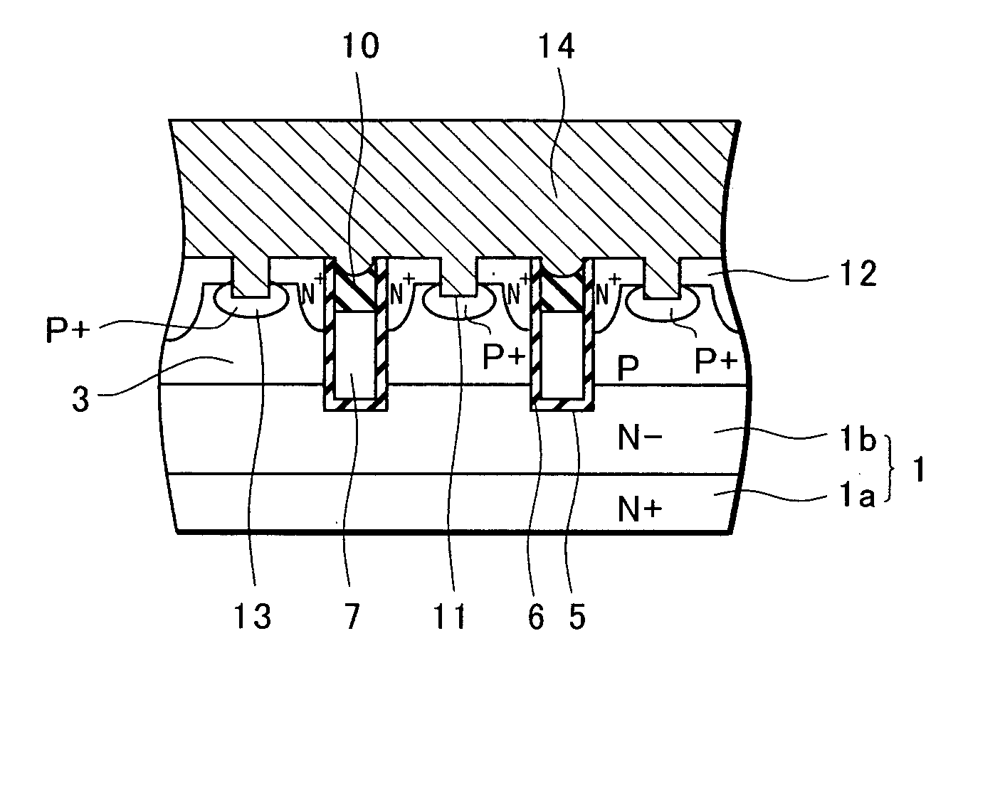
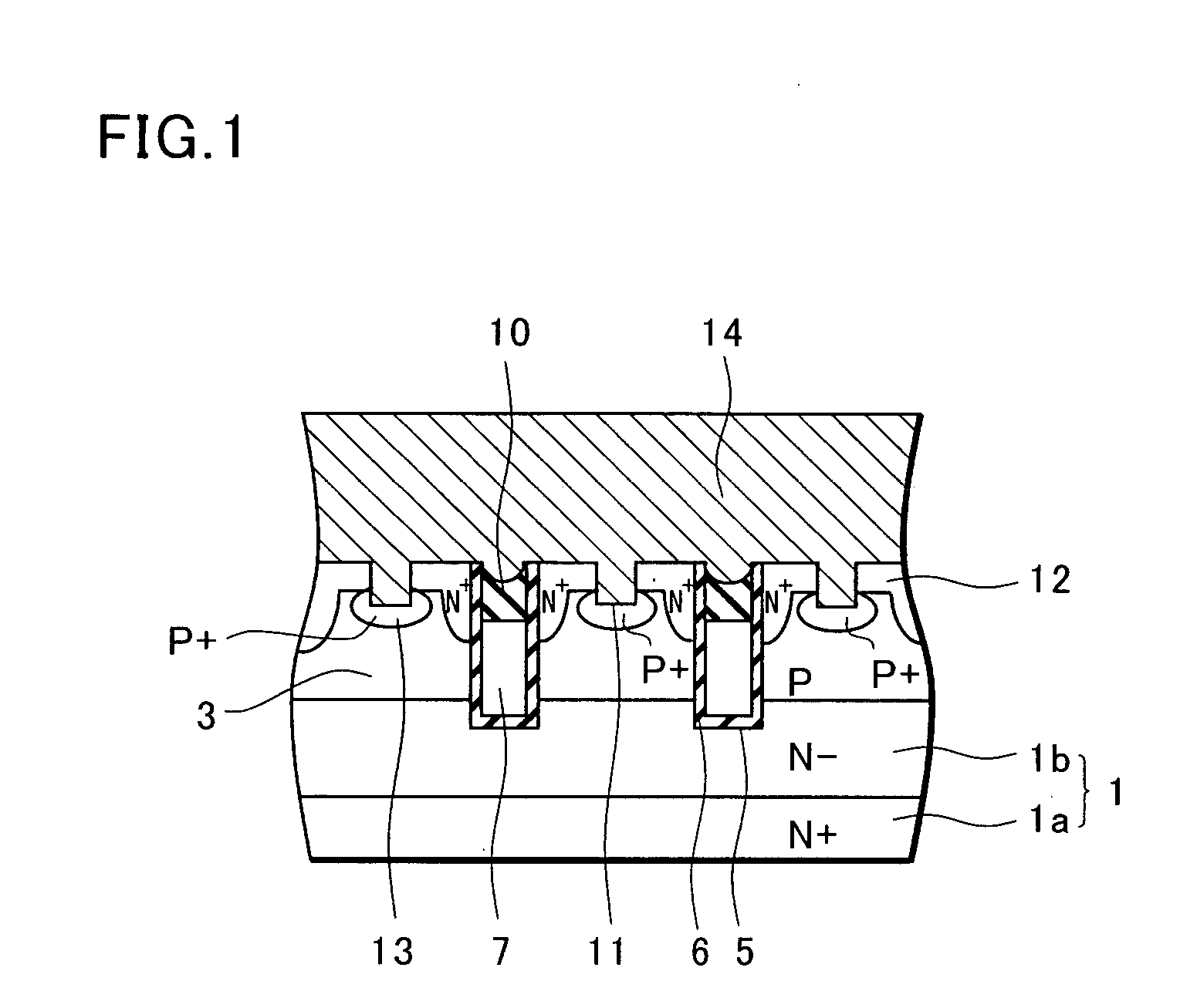
[0026]FIG. 1 shows a cross-sectional view of the MOSFET. The MOSFET includes a semiconductor substrate 1, a channel layer 3, a trench 5, a gate insulating film 6, a gate electrode 7, a source region 12, a body region 13, an interlayer dielectric film 10 and a source electrode 14.

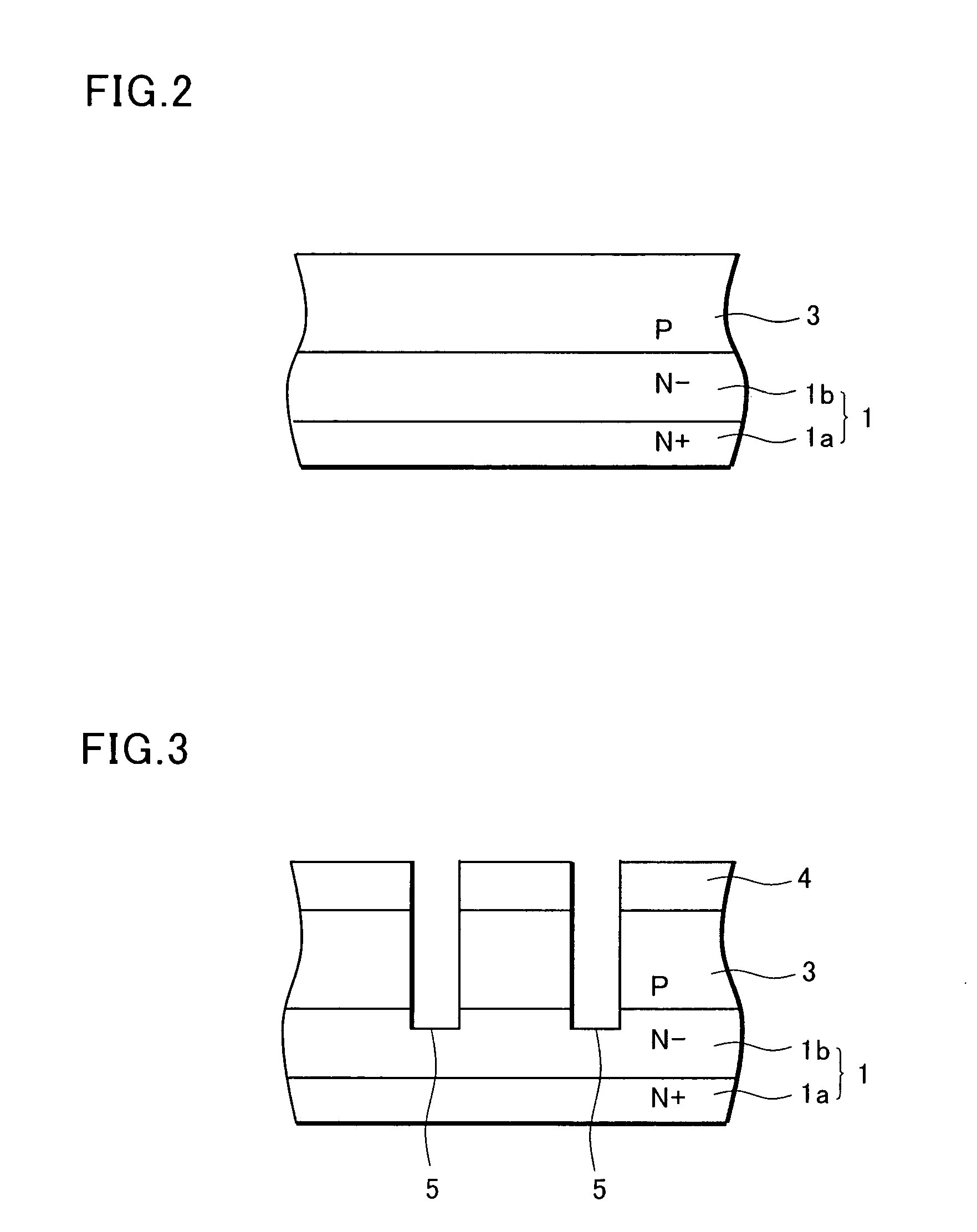
[0027] The semiconductor substrate includes an N+-type silicon semiconductor substrate 1a and an N−-type epitaxial layer 1b laminated thereon which forms a drain region. A channel layer 3 which is an opposite conductivity type impurity region is provided on a surface of the drain region 1b.

[0028] A trench 5 is formed so as to penetrate the channel layer 3 and to reach the drain region 1b, and is commonly patterned in stripes or lattice on a surface of the substrate. The inner wall of the trench 5 is covered with a gate insulating film 6 of several hundreds A according to...


PUM


Abstract

An interlayer dielectric film is completely buried in a trench, and failures caused by step coverage is prevented because a source electrode can be formed substantially uniformly on an upper portion of a gate electrode. Also, in the processes of forming a source region, a body region and an interlayer dielectric film, only one mask is necessary so that the device size is reduced to account for placement error of only one mask alignment.

Description

BACKGROUND OF THE INVENTION [0001] 1. Field of the Invention: [0002] The invention relates to an insulated gate-type semiconductor device and a method of manufacturing the same, specifically to an insulated gate-type semiconductor device with improved step coverage of a source electrode and a manufacturing method thereof. [0003] With insulated gate-type semiconductor devices like a MOSFET, the cell density is improved to achieve a low on resistance by using a trench structure. [0004] 2. Description of the Related Art: [0005]FIG. 9 shows an example of an N-channel type power MOSFET structure with a conventional trench structure. A drain region 21b is provided, for instance by laminating an N−-type epitaxial layer on an N+-type silicon semiconductor substrate 21a. A P-type channel layer 24 is formed on a surface of the drain region 21b. A trench 27 is provided which penetrates the channel layer 24 to reach the drain region 21b and inner walls thereof are covered with a gate oxide film...

Claims


Application Information

Patent Timeline
IPC IPC(8): H01L21/265H01L29/417H01L21/336H01L29/08H01L29/41H01L29/423H01L29/49H01L29/72H01L29/739H01L29/76H01L29/78
CPCH01L21/26586H01L29/0869H01L29/7813H01L29/66727H01L29/66734H01L29/4236H01L29/72
Inventor ONDA, MASAHITOKUBO, HIROTOSHIMIYAHARA, SHOUJIISHIDA, HIROYASUSAITO, HIROAKI
Owner SEMICON COMPONENTS IND LLC
Why Eureka
Try Eureka