
Buffer for temperature compensated crystal oscillator signals

a technology of temperature compensation and crystal oscillator, which is applied in the direction of oscillator generators, amplifiers with semiconductor devices/discharge tubes, instruments, etc., can solve the problems of high pressure to build electronic devices at a very low price, and generally more expensive than normal crystal oscillators

Active Publication Date: 2011-09-22
TEXAS INSTR INC
View PDF13 Cites 2 Cited by
  • Summary
  • Abstract
  • Description
  • Claims
  • Application Information

AI Technical Summary

Benefits of technology

[0004]It is an object of the invention to provide an electronic device for buffering temperature compensated crystal oscillator signals, which is configured to provide a limited damping, an acceptable fan-out and the capability to process signals with a limited voltage swing.
[0005]According to an aspect of the invention, an integrated semiconductor electronic device with a substrate having a first doping concentration is provided. The first doping concentration is a light doping, which means the concentration is for example about 108 / cm2 or between 107 / cm2 and 109 / cm2. There is a first MOS transistor configured to receive an output signal of a temperature compensated crystal oscillator (TCXO) at a control gate for providing the buffered TCXO signal at an output node. The output node may be the source of the first MOS transistor. This means that the first MOS transistor is configured to buffer the TCXO output signal. There is a second MOS transistor, which is built in a well having a second doping concentration. The well is built in the substrate with the first doping concentration. The second MOS transistor will then be coupled to supply a current to the first MOS transistor. The channel of the first MOS transistor is directly built in the substrate. The first doping concentration may be by at least a factor of ten lower than the second doping concentration. The second doping concentration may be about 1014 / cm2. The electronic device according to this aspect of the invention uses a specific MOS transistor (the first MOS transistor) in order to buffer the TCXO output signals. This MOS transistor is built in the lightly doped substrate without using a separate well. Due to these technological measures, it is possible to buffer signals, as for example the TCXO output signals having a low voltage swing and providing very limited damping and additive noise to the signals.
[0007]According to still another aspect of the invention, the first MOS transistor comprises a plurality of parallel branches. Each of the branches contains a partial MOS transistor. All the partial MOS transistors form together the first MOS transistor. The gates of the partial MOS transistors are coupled together to receive the output signal of the TCXO. There is further a plurality of resistors. There is one resistor coupled to each source of a partial MOS transistor. The other side of the resistors is coupled to the output node. This provides that the output resistance of the first MOS transistor is substantially reduced. Furthermore, also the noise characteristic of the first MOS transistor is reduced.
[0009]The electronic device according to the invention can be used to buffer signals from temperature compensated crystal oscillators (TCXOs). Therefore, electronic devices using this kind of buffer can substantially reduce the number of separate temperature compensated crystal oscillators. This reduces the overall costs of the respective devices and complexity.

Problems solved by technology

These crystal oscillators (i.e., 102-1 to 102-4) are generally more expensive than normal crystal oscillators due to their high stability and precision.
However, due to competition in the market, there is a very high pressure to build the electronic devices at a very low price.

Method used


Image

  • Buffer for temperature compensated crystal oscillator signals
  • Buffer for temperature compensated crystal oscillator signals
  • Buffer for temperature compensated crystal oscillator signals

Examples


Embodiment Construction

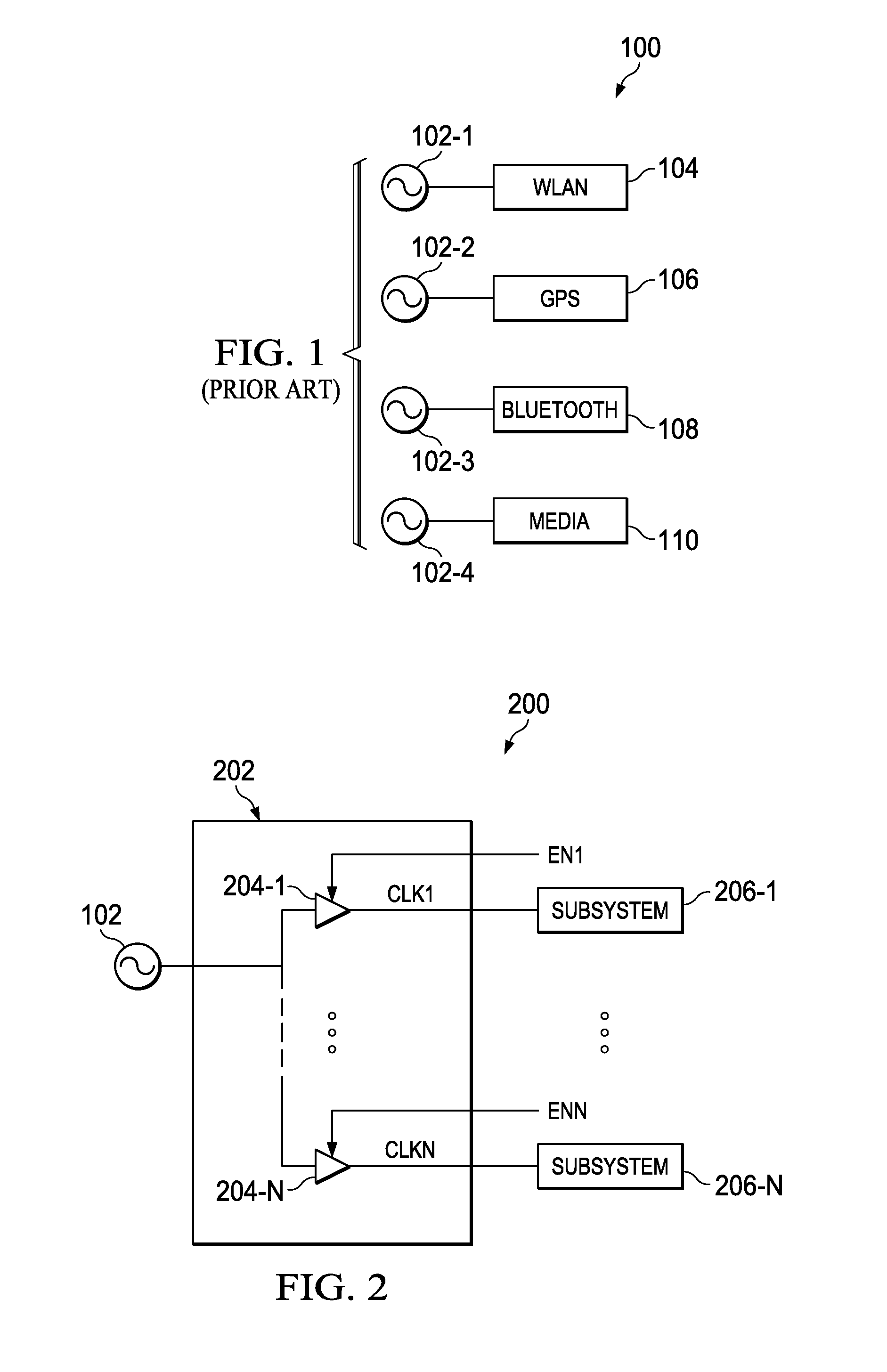
[0017]In FIG. 2, a system 100 in accordance with a preferred embodiment of the present invention can be seen. The system 100 generally comprises a TXCO 102, a clock distributor 202 (which generally includes clock buffers 204-1 to 204-N), and subsystems 206-1 to 206-N. These subsystems 206-1 to 206-N can generally correspond to features (i.e., Bluetooth subsystems) that use precision clock signals CLK1 to CLKN, which can be provided when buffers 204-1 to 204-N are enabled by enable signals EN1 o ENN.

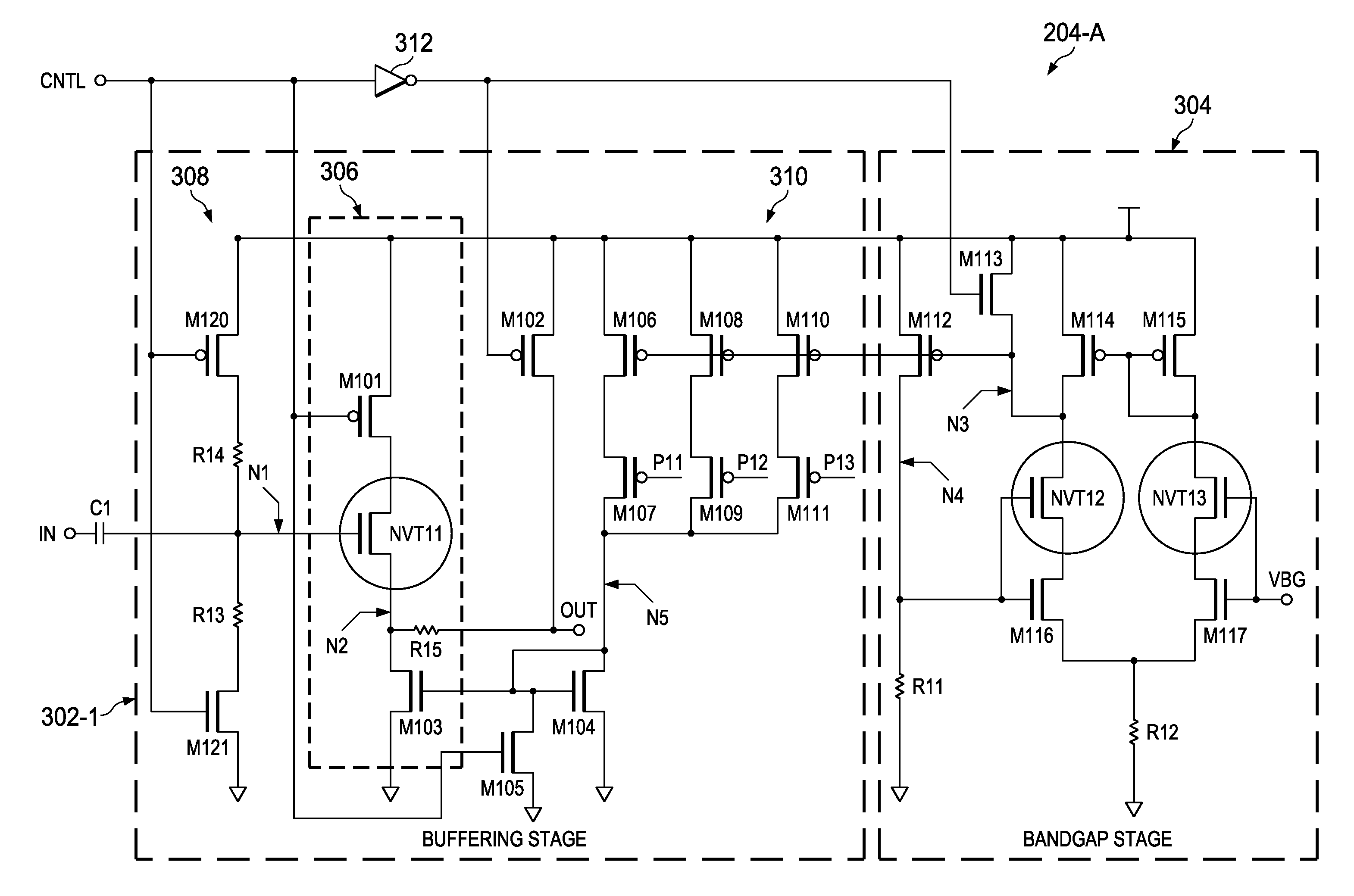
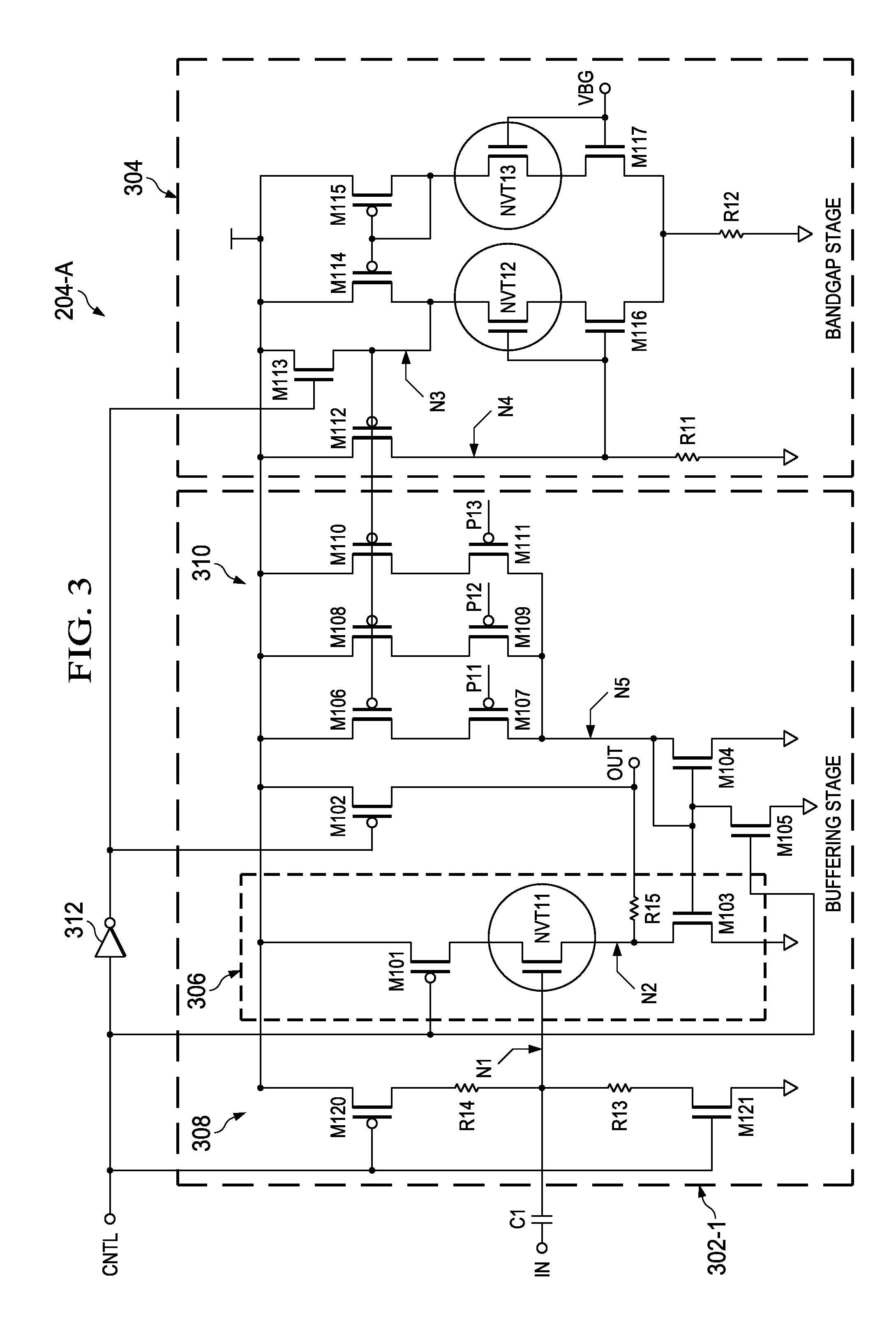
[0018]Turning now to FIG. 3, the clock buffers 204-1 to 204-N (hereinafter 204-A for FIG. 3) can be seen in greater detail. The clock buffer 204-A generally comprises a buffering stage 302-1 and a bandgap stage 304. At pin IN a signal from a TCXO (i.e., TXCO 102 of FIG. 1) is received. This signal passed through a decoupling or AC coupling capacitor C1 that may be implemented externally to the integrated circuit or IC. At pin CNTL an enable signal (i.e., EN1) is receives so as to enable o...


PUM


Abstract

A buffer is provided. The buffer includes a buffering stage that receives an enable signal and an input signal and that provides an output signal and a bandgap stage that is coupled to the buffering stage and that is activated and deactivated by the enable signal. In particular, the buffering stage includes a buffering substage that includes a buffering transistor that is coupled to the input stage, wherein the buffering transistor is formed on a substrate, and wherein the buffering transistor has a channel with a doping concentration that is approximately the same as the substrate.

Description

CROSS-REFERENCE TO RELATED APPLICATIONS[0001]This application is claims priority from German Patent Application No. 10 2010 011 757.9, filed Mar. 17, 2010, which is hereby incorporated by reference for all purposes.TECHNICAL FIELD[0002]The invention relates to an electronic device for buffering a signal of a temperature compensated crystal oscillator and a method for manufacturing such a device.BACKGROUND[0003]Along with the increasing popularity of handheld devices such as smart phones, PDAs and UMPCs etc. more and more functionality is to be integrated into a single portable device. A typical example of such a device is a mobile phone (also referred to as smart phones or media phones) which incorporate functions like Global Positioning System (GPS), wireless local area networks (WLAN), and Bluetooth. Typically, each of these features uses high performance stable clock signals. These clock signals are typically generated by temperature compensated crystal oscillators or TCXO, and f...

Claims


Application Information

Patent Timeline
IPC IPC(8): G05F3/16
CPCH03F3/505
Inventor SAREEN, PUNEET
Owner TEXAS INSTR INC
Learn More