Pixel circuit
a pixel circuit and circuit technology, applied in the field of pixel circuits, to achieve the effect of improving the overall performance of the pixel circuit and increasing the voltage swing of the read-out signal
- Summary
- Abstract
- Description
- Claims
- Application Information
AI Technical Summary
Benefits of technology
Problems solved by technology
Method used
Image
Examples
Embodiment Construction
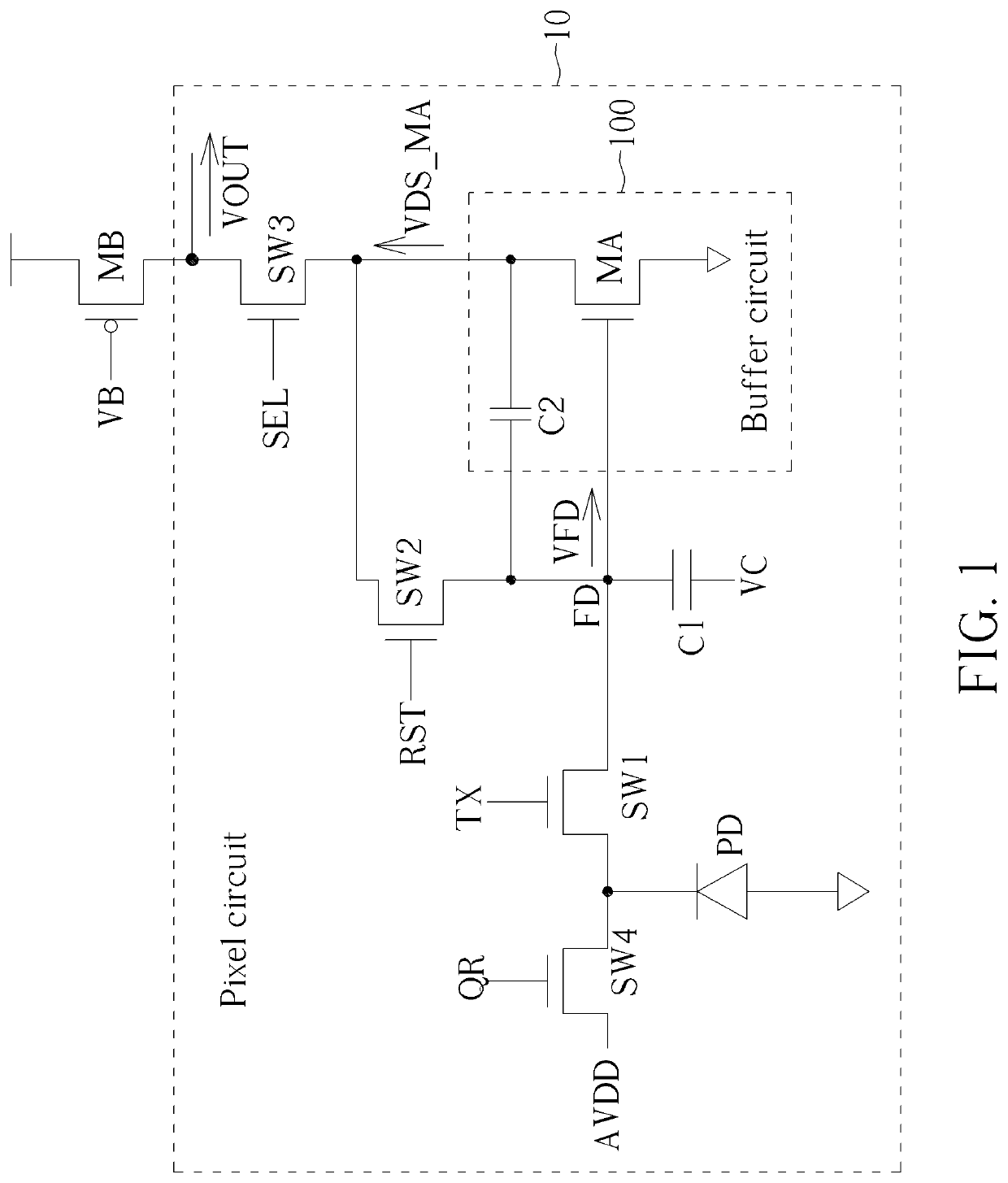
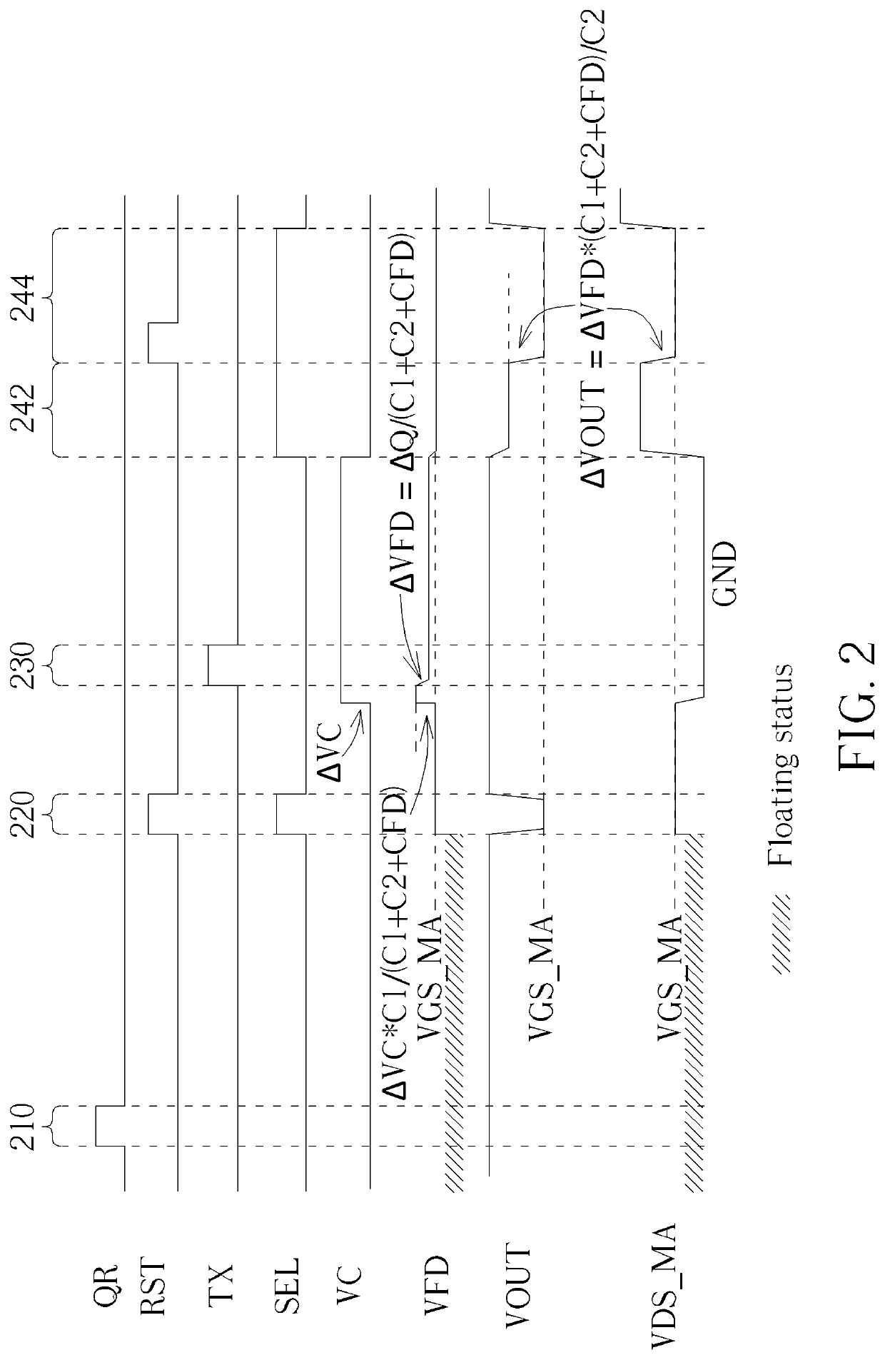
[0009]FIG. 1 is a diagram illustrating a pixel circuit 10 according to an embodiment of the present invention. As shown in FIG. 1, the pixel circuit may comprise a photodiode PD, a buffer circuit 100, a capacitor C1, a switch SW1, a switch SW2 and a switch SW3. The photodiode PD is configured to accumulate charges (e.g. electrons) in response to incident radiation, to generate a photodiode signal. The buffer circuit 100 is configured to output at least one read-out signal, wherein an input terminal of the buffer circuit 100 is coupled to a specific node (e.g. a floating diffusion node) such as a node FD, and a signal on the node FD is represented by a signal VFD. The capacitor C1 is coupled between a control voltage terminal (controlled by a signal VC) of the pixel circuit 10 and the node FD. The switch SW1 is coupled between the photodiode PD and the node FD. The switch SW2 is coupled between the input terminal of the buffer circuit 100 and an output terminal of the buffer circuit ...
PUM
| Property | Measurement | Unit |
|---|---|---|
| voltage level | aaaaa | aaaaa |
| bias current | aaaaa | aaaaa |
| voltage | aaaaa | aaaaa |
Abstract
Description
Claims
Application Information

