A preparation method of gan E/D integrated device based on secondary oxidation method

A technology of secondary oxidation and integrated devices, which is applied in semiconductor/solid-state device manufacturing, electric solid-state devices, semiconductor devices, etc. Process consistency and controllability are not high, etching damage reduces device saturation current, etc., to achieve high process stability and consistency, low interface state density, and good on-chip consistency.

Active Publication Date: 2018-03-20
NO 55 INST CHINA ELECTRONIC SCI & TECHNOLOGYGROUP CO LTD
View PDF3 Cites 0 Cited by
  • Summary
  • Abstract
  • Description
  • Claims
  • Application Information

AI Technical Summary

Problems solved by technology

[0004] On the one hand, based on the depletion device material structure, the traditional gate trenching process is used to realize the enhanced device. The original barrier layer thickness (about 20-30nm) needs to be thinned to less than 5nm, and the controllability of the barrier layer deep trenching process And repeatability is difficult to guarantee, and it will inevitably bring etching damage, which will reduce the saturation current of the device and increase the gate leakage; and the fluorine ion implantation technology also has low process consistency and controllability, and fluorine ion mobility at high temperature The resulting device reliability problems make it difficult to meet the needs of large-scale applications
On the other hand, the design of the new intrinsic enhancement material structure can better control the threshold voltage of the enhancement device and improve the consistency of the device. At present, it has become the mainstream method for preparing a single enhancement device. However, due to the limitation of the material structure itself, Incompatible with the material structure requirements of E and D-mode devices, it is not suitable for E / D integration. For example, in the E / D integrated circuit developed by HRL laboratory, different material structures are used for E-mode devices and D-mode devices. , to obtain intrinsic enhancement-mode devices and depletion-mode devices

Method used


Image

  • A preparation method of gan E/D integrated device based on secondary oxidation method
  • A preparation method of gan E/D integrated device based on secondary oxidation method
  • A preparation method of gan E/D integrated device based on secondary oxidation method

Examples


preparation example Construction

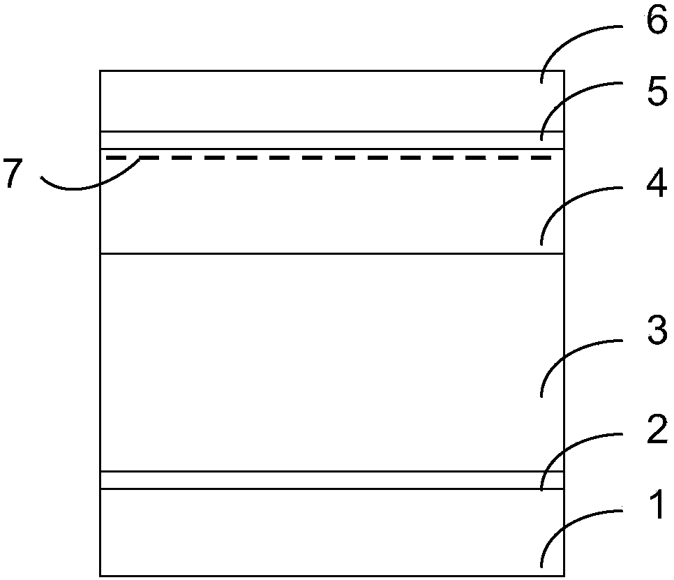
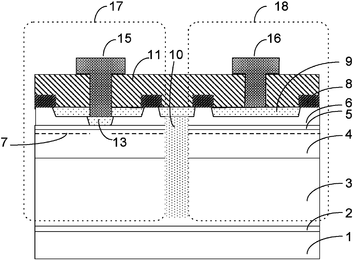
[0026] like Figures 1~3 As shown, a method for preparing a GaN E / D integrated device based on a secondary oxidation method, the preparation steps of which include the following steps:

[0027] a) A nucleation layer 2, an AlyGa1-yN buffer layer 3, a GaN channel layer 4, an AlN insertion layer 5, and a barrier layer 6 are sequentially grown on the substrate 1 to form a GaN HEMT heterostructure, and the hetero interface forms a two-dimensional electronic gas 7;

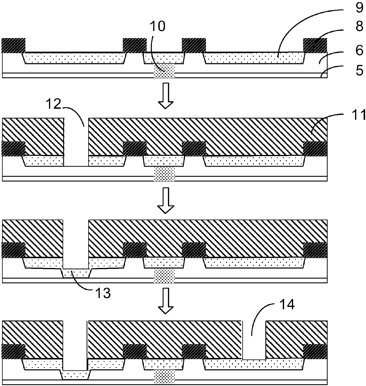
[0028] b) After the conventional ohmic metal electrode 8 is completed, the oxygen plasma treatment method is used for the first oxidation, which consumes part of the barrier layer 6 and reduces its thickness to half of the original thickness, and at the same time generates a first layer of oxide medium 9 on the surface; this The two-dimensional electron gas 7 is still retained in the channel;

[0029] c) Perform device isolation 10, make a mask 11, open holes in the area 12 reserved for making the gate feet of the E-m...

Embodiment 1

[0034] AlN nucleation layer 2 is grown on SiC substrate, 1μm GaN is grown as buffer layer 3, 40nm undoped GaN is used as channel layer 4, 1.5nm AlN insertion layer 5, and finally 6nm undoped Al0.72In0.18N is covered. barrier layer 5, in which the concentration of two-dimensional electron gas 7 is 1.87×10 13 cm -2, constituting an AlInN / AlN / GaN heterostructure material for E / D integration. After the conventional ohmic metal electrode 8 is completed, the first oxidation treatment is carried out. This oxidation condition can consume the 3nm Al0.72 In0.18N barrier layer 5 to generate the first layer of oxide medium 9, and then use the B ion implantation method to carry out Isolate 10, make a mask 11, open a window by photolithography in the area 12 reserved for making the gate foot of the E-mode device, remove the gate foot dielectric 9 of the E-mode device, and then perform a second oxidation, and the oxidation conditions are the same as the first oxidation conditions. It is ex...

Embodiment 2

[0036] AlN nucleation layer 2 is grown on the SiC substrate, 1μm Al0.08Ga0.92N is grown as buffer layer 3, 20nm undoped GaN is grown as channel layer 4, 2nm AlN insertion layer 5, and finally 4nm undoped Al0 is covered. 5Ga0.5N barrier layer 5, in which the concentration of two-dimensional electron gas 7 is 1.32×10 13 cm -2 , constituting an AlGaN / AlN / GaN heterostructure material for E / D integration. After the conventional ohmic metal electrode 8 is completed, the first oxidation treatment is carried out. This oxidation condition can consume the 2nm Al0.5Ga0.5N barrier layer 5 to generate a first layer of oxide medium 9, and then use B ion implantation for isolation. 10. Make a mask 11, open a window by photolithography in the area 12 reserved for making the gate foot of the E-mode device, remove the gate foot dielectric 9 of the E-mode device, and then perform a second oxidation. The oxidation conditions are completely the same as the first oxidation conditions. The same, t...


PUM


Abstract

The invention discloses a method for preparing a GaN E / D integrated device based on a secondary oxidation method. Based on the traditional depletion-type AlGaN (AlInN) / AlN / GaN heterostructure, the oxidation method is used to precisely control the thickness of the barrier layer. Oxidation thins the barrier layer to half of its original thickness, and the channel still maintains a high concentration of two-dimensional electron gas. The dielectric generated by oxidation is used as the gate dielectric of the D-mode device; then the dielectric in the gate foot area of ​​the E-mode device is removed, and then the second The secondary oxidation completely consumes the barrier layer, depletes the two-dimensional electron gas in the channel, and generates the gate foot dielectric of the E-mode device at the same time. The two oxidation processes are the same, so that the E and D-mode device processes are fully compatible and the thickness of the gate dielectric is the same. It ensures that the device structure matches the device performance. The invention adopts an oxidation method to thin the barrier layer to realize the preparation of the E-mode device, and the process is highly controllable; the E-mode and D-mode processes are fully compatible, and the gate dielectrics of the E and D-mode devices have the same thickness and performance matching, which is beneficial to improve the GaN E / D integrated circuit yield.

Description

technical field [0001] The invention relates to the technical field of semiconductor field effect transistors and their integrated circuits, in particular to a preparation method of a GaN E / D integrated device based on a secondary oxidation method. Background technique [0002] In recent years, with the practical development of GaN microwave power devices, the application of GaN materials in high-speed digital and mixed-signal circuits has attracted more and more attention, aiming to give full play to its high electron drift speed and high breakdown voltage. Advantages, to obtain ideal voltage swing while maintaining high-speed performance, to cope with the rapid decline of Si-based integrated circuit breakdown voltage as device size shrinks. Especially in the past two years, GaN high-frequency device and E / D integration research has gradually become an international research hotspot, and is called the next-generation GaN electronic device and integrated circuit technology. ...

Claims


Application Information

Patent Timeline
Patent Type & Authority Patents(China)
IPC IPC(8): H01L27/06H01L29/78H01L21/28H01L21/8248
Inventor 孔月婵周建军孔岑
Owner NO 55 INST CHINA ELECTRONIC SCI & TECHNOLOGYGROUP CO LTD
Why Eureka
Try Eureka