Method for forming a variable thickness dielectric stack

a dielectric stack and variable thickness technology, applied in the direction of semiconductor devices, basic electric elements, electrical equipment, etc., can solve the problems of device processing, difficult to perform transistor component alignment across typical substrate widths up to one meter or more, and the impact of traditional photolithographic processes and equipmen

Inactive Publication Date: 2016-05-05
EASTMAN KODAK CO
View PDF0 Cites 10 Cited by
  • Summary
  • Abstract
  • Description
  • Claims
  • Application Information

AI Technical Summary

Benefits of technology

[0078]An advantage of the variable thickness dielectric layer 150 is that the size of the gate via 814 can be sized independently of the size and location of the other elements in the TFT 100. In prior art processes for forming transistors with variable thickness dielectric layers, the region of extra dielectric thickness between the overlap of the gate and source / drain layers is aligned, and most often self-aligned, with the source and drain. This use of an aligned structure results in the dielectric thickness immediately adjacent the channel region being thicker than the gate dielectric thickness in the channel. As a consequence, prior art uses of extra dielectric thickness in the overlap between the gate and the source / drain have been limited to top gate architectures. This limitation is a functional limitation; if a self-aligned extra dielectric portion was used in a bottom gate architecture, it would prevent good charge injection into the semiconductor since the region of contact of the source and drain with the semiconductor would be separated from the gate by a dielectric having a thickness greater than the gate dielectric thickness. Another advantage of the present invention is that the variable thickness dielectric layer 150 can be implemented in any TFT architecture—bottom gate or top gate, with or without staggered contacts.
[0079]FIG. 2 is a cross-sectional diagram of an alternative embodiment of a TFT 102 of the present invention, taken along the line A-A′ of the plan view shown in FIG. 1b. The TFT 102 shown in FIG. 2 is a bottom gate structure similar to TFT 100 shown in FIG. 1a, and also has a gate 120 in contact with the substrate 110 and a variable thickness dielectric stack 152. The variable thickness dielectric stack 152 is in contact with the gate 120, the substrate 110, and the semiconductor layer 170. The semiconductor layer 170 is in contact with the source electrode 180 and the drain electrode 185. The substrate 110, gate 120, semiconductor layer 170, and source and drain electrode 180,185 should be understood from the previous description of FIGS. 1a and 1b.
[0080]The variable thickness dielectric stack 152 shown in FIG. 2 serves the same function and has the same defining features as the variable thickness dielectric stack 150 shown in FIG. 1a. The dielectric stack 152 is in contact with the gate 120 and has first, second, and third regions, where the first region is in contact with the semiconductor layer 170 in the channel region and has a first thickness, the second region is adjacent to the first region and also has the first thickness, and the third region that is adjacent to the second region having a second thickness greater than the first thickness. As discussed with respect to FIG. 1a, this feature of variable thickness provides a thicker dielectric where the source and drain electrodes 180, 185 overlap the much of gate 120, including the gate edge, reducing the potential for shorting and decreasing the gate leakage. The thinner dielectric over the gate 120 in the channel region of the device controls the electrical field experienced in the semiconductor layer 170 when the gate 120 is activated. The additional dielectric buffer layer 160 in dielectric stack 152 serves to control the interface between the semiconductor layer 170 and the gate dielectric 152, which is known to be critical to the function of the TFT 102. In TFTs that are formed by the combination of SAD and ALD, special care should be taken to insure that the interface between the semiconductor and the gate dielectric is not disturbed by the removal of the deposition inhibiting material. As shown in FIG. 2, the dielectric buffer layer 160 has the same pattern as the semiconductor layer 170 and is in contact with the semiconductor layer 170. The additional dielectric buffer layer 160 can be a different material from the other layers in the variable thickness dielectric stack 152. Preferably, all of the layers of the variable thickness dielectric stack 152, including the additional dielectric buffer layer 160, have the same material composition. As discussed above, although each layer is formed of the same material, when the layers are formed in separate steps the interfaces between the layers can be detected by a change in the intensity signal of either an impurity or compositional species.
[0081]Variable thickness dielectric stack 152 is made up of patterned first inorganic dielectric layer 130, patterned second dielectric layer 140, and the additional dielectric buffer layer 160. The first inorganic thin film dielectric layer 130 has a first pattern and the second inorganic thin film dielectric layer 140 has a second pattern. As shown in FIGS. 1a and 1b, the first pattern of the first dielectric layer 130 includes a portion having a via 814 over the gate 120 in the channel region of the device (the via indicates that layer 130 has no appreciable thickness) and other portions of the pattern between the source and drain electrodes 180,185 and the gate electrode 120 have a larger thickness. The second inorganic thin film dielectric layer 140 has a pattern that is different from that of the first pattern, and has a uniform thickness over the gate, both in the area where the source and drain electrodes 180,185 overlap the gate 120 and within the channel region of the TFT 102. The additional dielectric buffer layer 160 has a uniform thickness in the area of the semiconductor pattern. Plainly stated, the variable thickness dielectric stack 152 provides a gate dielectric thickness that is thinner than the dielectric thickness in much of the overlap region between the source and drain electrodes 180,185 and the gate 120. Additionally, the thinnest portion of the dielectric stack in the channel region can be independently sized from the other portions of the dielectric stack 152. It is preferable that, as shown, there is a second region adjacent to the channel having the same thickness as the gate dielectric within the channel region to ensure that the source and drain electrodes 180,185 contact the semiconductor layer 170 in a region of proper dielectric thickness; as shown in FIG. 2 this thickness is equal to the combined thickness of the second dielectric layer 140 and the additional dielectric buffer layer 160. This extension of the gate dielectric thickness region beyond the channel region defined by the gap between the source and drain electrodes 180,185 enables good charge injection and also robust alignment when fabricating the TFT 102 shown in FIGS. 2 and 1b. In alternative embodiments, the first patterned dielectric layer 130 is formed in contact with the additional dielectric buffer layer 160, and the second patterned inorganic thin film dielectric layer 140 is formed in contact with the substrate 110. This reversal of order of the first and second thin film dielectric layer results 130, 140 in an equivalent variable thickness dielectric stack 152.
[0082]FIG. 3 is a cross-sectional diagram of an alternative embodiment of a TFT 103 of the present invention, taken along the line A-A′ of the plan view shown in FIG. 1b. The TFT 103 shown in FIG. 3 is a bottom gate structure similar to TFT 100 shown in FIG. 1a, and also has a gate 120 in contact with the substrate 110, and has a variable thickness dielectric stack 153. The variable thickness dielectric stack 153 is in contact with the gate 120, the substrate 110, and the semiconductor layer 170. The semiconductor layer 170 is in contact with the source electrode 180 and the drain electrode 185. As shown in FIG. 3, the substrate 110, gate 120, semiconductor layer 170, and source and drain electrode 180,185 should be understood from the previous description of FIGS. 1a and 1b.
[0083]The TFT 103 of FIG. 3 illustrates an embodiment of the present invention wherein the interface between the dielectric layer 153 and the semiconductor layer 170 is controlled by dielectric buffer layer 143, and the thickness of the dielectric buffer layer 143 is the same as the thickness of the gate dielectric in the channel region. The first inorganic thin film dielectric layer 130 has a first pattern and the dielectric buffer layer 143 has a second pattern. In the embodiment of TFT 103, the dielectric buffer layer 143 is a second patterned dielectric layer. The first pattern of the first dielectric layer 130 includes a portion over the gate in the channel region of the device with no thickness (i.e. gate via 814), and other portions of the pattern between the source and drain electrodes 180,185 and the gate electrode 120 having a larger thickness. The dielectric buffer layer 143 has a second pattern that is different from that of the first pattern and has a uniform thickness in the area between the source and drain electrodes 180, 185 and the gate 120 within the channel region of the TFT 103. As shown in FIG. 3, the second pattern is the same as the pattern of the semiconductor layer 170. The combination of the patterns of first and second thin film dielectric layers 130, 143 form a dielectric stack 153 in contact with the gate 120 having first, second, and third regions, the first region in contact with the semiconductor layer 170 in the channel region and having a first thickness, the second region adjacent to the first region having the first thickness, and the third region adjacent to the second region having a second thickness greater than the first thickness. Plainly stated, the dielectric stack 153 provides a gate dielectric thickness in the channel region that is thinner than the dielectric thickness in much of the overlap region between the source and drain electrodes 180,185 and the gate 120.

Problems solved by technology

Plastics, however, typically limit device processing to below 200° C. There are other many issues associated with plastic supports when using traditional photolithography during conventional manufacturing, making it difficult to perform alignments of transistor components across typical substrate widths up to one meter or more.
Traditional photolithographic processes and equipment may be seriously impacted by the substrate's maximum process temperature, solvent resistance, dimensional stability, water, and solvent swelling, all key parameters in which plastic supports are typically inferior to glass.
There persists a problem of combining multiple SAD steps to form working devices.
This required layer thickness typically requires long processing times and limits the functionality of field effect devices.
In CMOS circuitry, inverters are typically easy to design but disadvantageously expensive to produce and utilize complicated production processes.
It is possible to build all NMOS or PMOS inverters, however particularly for enhancement-depletion mode circuits there are challenges to independently controlling the behavior of each transistor in the inverter circuit.
Typically, the depletion mode transistor will have a thicker semiconductor layer than the enhancement mode transistor, increasing process complexity and increasing cost.
Other alternatives include using dual gate architectures or multilayer semiconductor stacks, which have similar issues of process complexity and cost.

Method used


Image

  • Method for forming a variable thickness dielectric stack
  • Method for forming a variable thickness dielectric stack
  • Method for forming a variable thickness dielectric stack

Examples


examples

General Conditions for the Preparation of Layers Using Atmospheric Pressure ALD

[0130]The preparation of a thin film coating of the material layers on glass substrates as used in the examples is described below. The ALD coating device used to prepare these layers, namely aluminum oxide, ZnO:N, and Al-doped ZnO (AZO), has been described in detail in US Patent Application Publication No. US 2009 / 0130858, the disclosure of which is herein incorporated by reference in its entirety. The coating device has an output face (facing up) that contains spatially separated elongated gas channels and operates on a gas bearing principle. The coating device can be understood with respect to delivery head 900 shown in FIG. 28. Each gas channel is composed of an output slot 95, 93, 92 which supplies gas to the output face 905, and adjacent exhaust slots 91 which remove gas from the output face 905. The order of the gas channels is P-O-P-M-P-O-P-M-P-O-P where P represents a purge channel, O represents ...

example i1

Inventive Example I1

Bottom Gate TFT with an Extra 500 Å Outside of the Channel Region

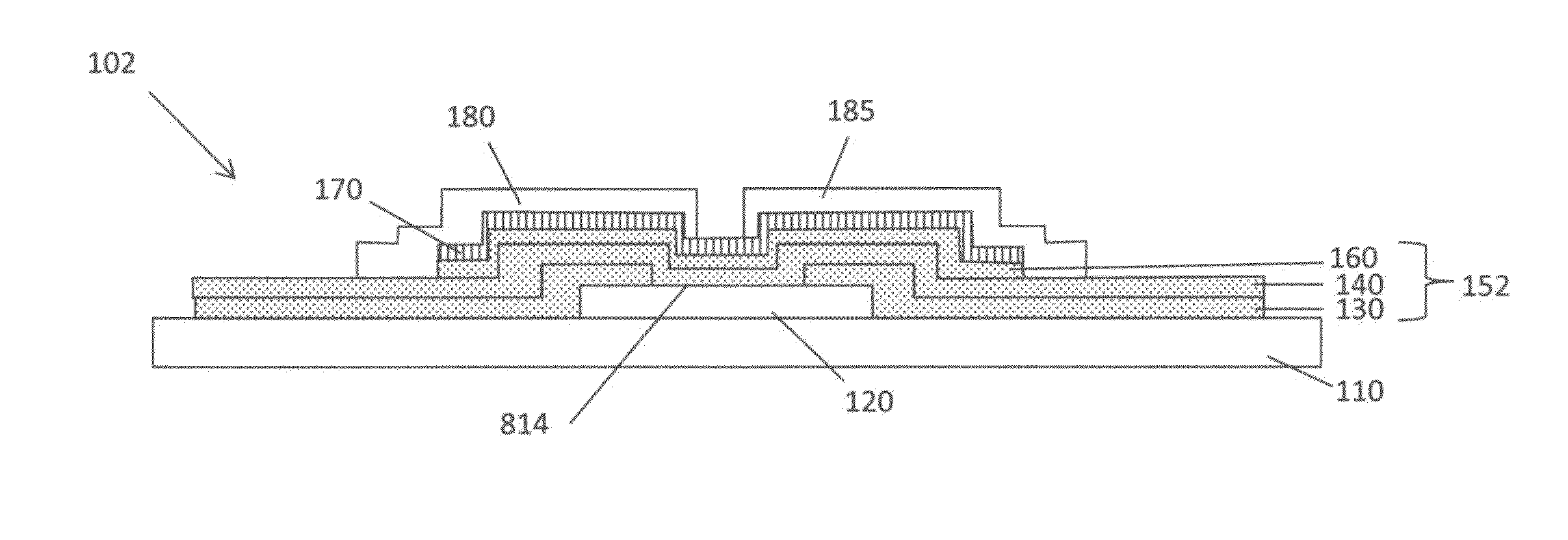
[0137]Inventive Example I1 is a bottom-gate transistor with the variable thickness dielectric stack of the present invention. Inventive Example I1 was fabricated as Comparative Example C1 with the following exceptions. After removing the PVP used to pattern the gate, a 500 Å extra dielectric layer having a gate via was formed using selective area deposition. The transistors were completed and characterized as in comparative example C1. The performance data for Inventive Example I2 can be found in the Id-Vg curve shown in FIG. 29.

[0138]As can be seen in FIG. 29, the inventive examples having the extra dielectric outside of the channel region perform similarly to the comparative example without the extra dielectric layer, having the same gate dielectric thickness within the channel region.

All-Enhancement-Mode Inverters

[0139]In order to further probe the usefulness of the variable thickness dielectric ...

example i6

Inventive Example I6

Enhancement-Depletion-Mode Inverter with Common Dielectric Stack

[0147]Inventive Example I6 was fabricated using the combination of spatial ALD and selective area deposition (SAD) on a glass substrate. A 200 Å ZnO:N semiconductor layer for the top gate load TFT was formed first, so that the back channel was in contact with the glass. Next, the first conductive layer containing the gate of the bottom gate drive TFT and the source and drain for the load TFT was formed using 1000 Å AZO. A 400 Å common dielectric layer was formed from two separately patterned 200 Å dielectric layers of Al2O3 to make the gate dielectric for the load TFT and a portion of the gate dielectric for the drive TFT. Next, a buffer layer and the semiconductor layer of the drive TFT were formed from a single inhibitor pattern with 100 Å of Al2O3 and 200 Å of ZnO:N. The second conductive layer containing the source and drain of the bottom gate drive TFT and the gate for the load TFT was formed us...


PUM

PropertyMeasurementUnit
widthsaaaaaaaaaa
drain currentaaaaaaaaaa
temperatureaaaaaaaaaa

Abstract

Producing a variable thickness dielectric stack includes providing a substrate with a first patterned conductive layer thereon. A first dielectric thin film is deposited using ALD and a first patterned deposition inhibitor layer, which is subsequently removed, to form a first patterned conformal dielectric layer having a first pattern. A second dielectric thin film is deposited using ALD and a second patterned deposition inhibitor layer to form a second patterned conformal dielectric layer having a second pattern. A second patterned conductive layer is formed with at least a portion of the first and second patterned conductive layers overlapping each other forming an overlap region. A portion of the first or second pattern extends into the overlap region such that one portion of the overlap region includes the first and second dielectric thin films, and another portion of the overlap region includes only the first or second dielectric thin film.

Description

CROSS REFERENCE TO RELATED APPLICATIONS[0001]Reference is made to commonly-assigned, U.S. patent application Ser. No. ______ (Docket K001871), entitled “TFT SUBSTRATE WITH VARIABLE DIELECTRIC THICKNESS”, Ser. No. ______ (Docket K001872), entitled “ENHANCEMENT-DEPLETION MODE INVERTER WITH TWO TRANSISTOR ARCHITECTURES”, Ser. No. ______ (Docket K001897), entitled “ENHANCEMENT MODE INVERTER WITH VARIABLE THICKNESS DIELECTRIC STACK”, all filed concurrently herewith.FIELD OF THE INVENTION[0002]This invention relates generally to patterned thin film fabrication and electronic and optoelectronic devices including patterned thin films. In particular, this invention relates to selective area deposition of materials including, for example, metal-oxides and devices including, for example, thin film transistors, inverters and circuits produced using, for example, this fabrication technique.BACKGROUND OF THE INVENTION[0003]Modern-day electronics require multiple patterned layers of electrically o...

Claims


Application Information

Patent Timeline
Patent Type & Authority Applications(United States)
IPC IPC(8): H01L21/28H01L21/02
CPCH01L21/0228H01L21/28158H01L21/02178H01L21/02554H01L21/02565H01L21/02579H01L21/0262H01L21/32H01L27/1225H01L29/42384H01L29/4908H01L29/66969H01L29/7869H01L29/78696H01L2029/42388
Inventor ELLINGER, CAROLYN RAE
Owner EASTMAN KODAK CO
Why Eureka
Try Eureka