Switching system capable of reducing noise of output signal
- Summary
- Abstract
- Description
- Claims
- Application Information
AI Technical Summary
Benefits of technology
Problems solved by technology
Method used
Image
Examples
Embodiment Construction
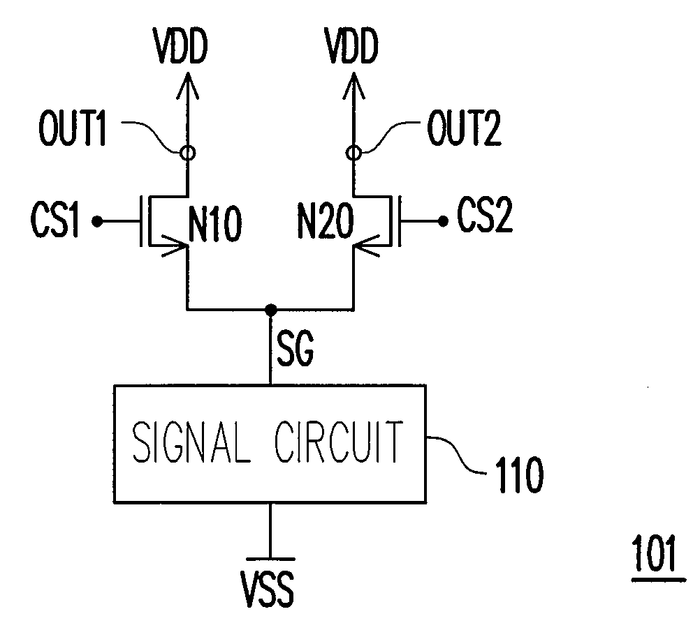
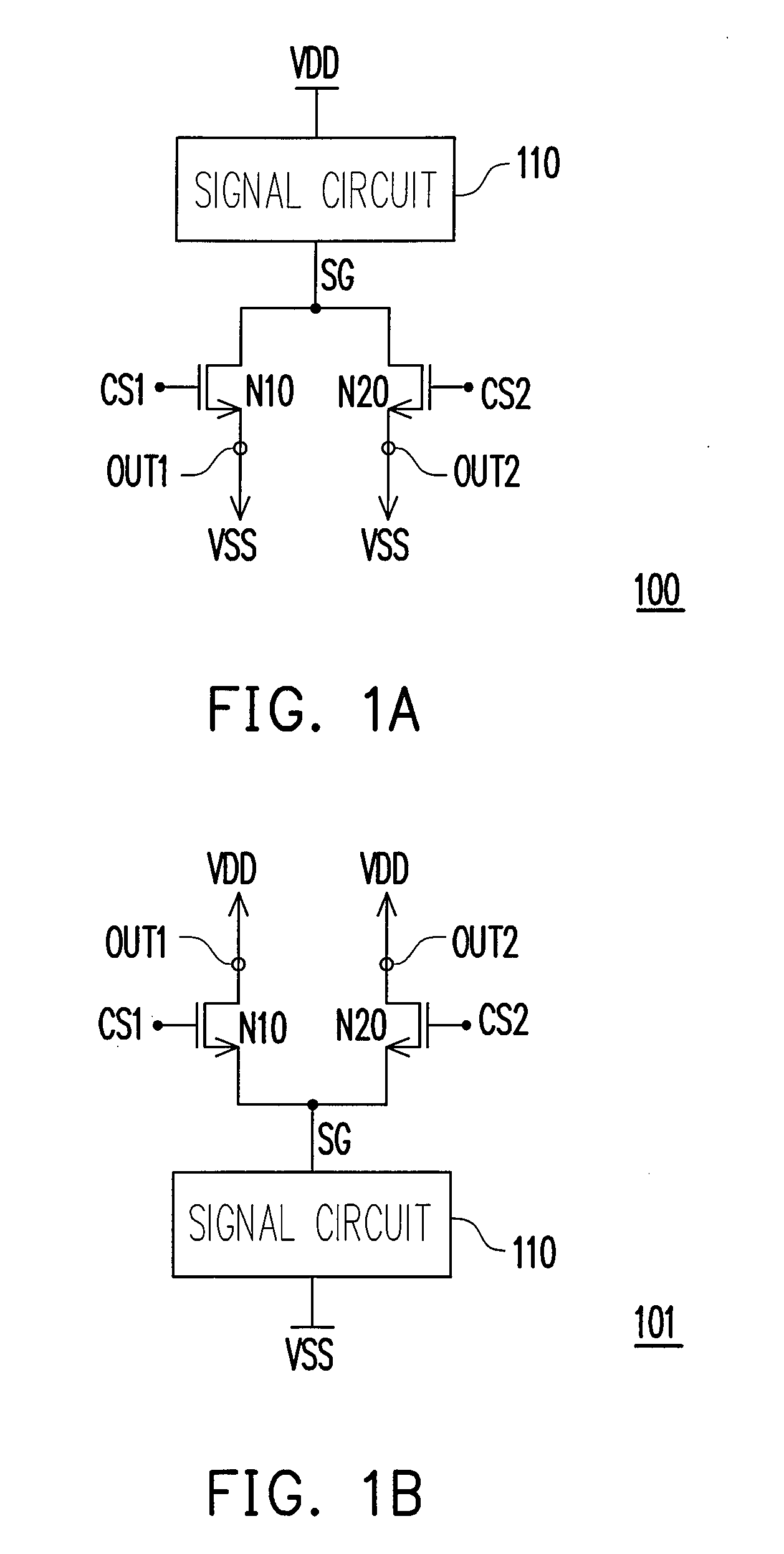
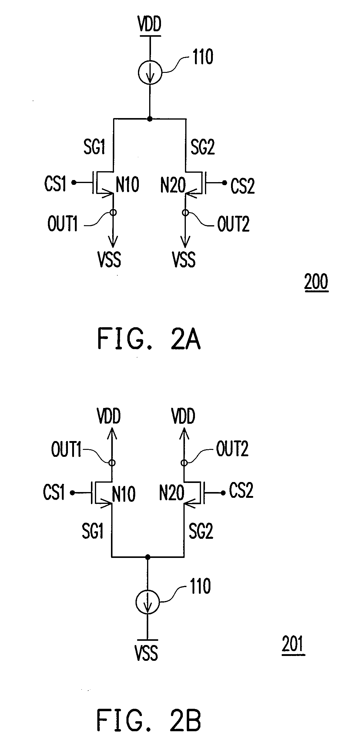
[0024]FIG. 1A is a schematic circuit diagram of a switching system according to an embodiment of the present invention. The switching system is suitable for converting current in a current mode DAC. The switching system 100 includes a signal circuit 110 and NMOS transistors N10 and N20, wherein the NMOS transistors N10 and N20 are comprised of, for example, N-type transistors and the signal circuit 110 is adapted for providing a signal SG. The NMOS transistor N10 is coupled between the first output terminal OUT1 of the switching system 100 and the signal SG, and the control terminal (gate) of the NMOS transistor N10 is coupled to a first control signal CS1. The NMOS transistor N20 is coupled between the second output terminal OUT2 of the switching system 100 and the signal SG, and the control terminal (gate) of the NMOS transistor N20 is coupled to a second control signal CS2. The first control signal CS1 and the second control signal CS2 are phase-inverted to each other. The NMOS t...
PUM
 Abstract
Description
Claims
Application Information


