Magnetic random access memory with stacked memory cells having oppositely-directed hard-axis biasing

a random access memory and memory cell technology, applied in the field of magnetic random access memory (mram), can solve the problems of severe degraded write-current margin and complicated fabrication process, and achieve the effect of reducing the switching field

Active Publication Date: 2007-10-23
INTELLECTUAL VENTURES HOLDING 81 LLC
View PDF23 Cites 57 Cited by
  • Summary
  • Abstract
  • Description
  • Claims
  • Application Information

AI Technical Summary

Benefits of technology

[0009]The invention is an MRAM with memory units or stacks arranged in the X-Y plane on the MRAM substrate with each memory stack having two memory cells stacked along the Z axis, and each memory cell having an associated biasing layer. Each biasing layer reduces the switching field of its associated cell by applying a biasing field along the hard-axis of magnetization of the free layer of its associated cell. The two cells in a stack are magnetically separated by a nonmagnetic separation layer. The free layers in the two cells in each stack have their in-plane easy axes of magnetization aligned parallel to one another. Each biasing layer has its in-plane magnetization direction oriented perpendicular to the easy axis of magnetization (and thus parallel to the hard axis) of the free layer in its associated cell. The hard-axis biasing fields generated by the two biasing layers are in opposite directions.
[0011]The oppositely-directed hard-axis biasing fields do not change the shape of the switching astroids of the cells, but merely shift the astroids in opposite directions along the hard-axis direction. Thus the two cells can have the same uniaxial anisotropies, which enables the two cells to have the same shape in the X-Y plane and be formed of the same ferromagnetic materials with the same thicknesses. For this reason the same value of write current can be applied along both write lines to switch the magnetic states of the cells. Thus the MRAM write circuitry does not need to be capable of generating multiple levels or amplitudes of write current. The hard-axis biasing fields assist the write field, reducing the switching threshold. Thus less write current is required, which reduces the power consumption of the MRAM.

Problems solved by technology

If it was desired to have the two cells have the same shape, then different ferromagnetic materials would have to be used for the two cells to create the different anisotropies, which would complicate the fabrication process.
A problem arises in an MRAM that has memory units of multiple stacked memory cells because as the units become densely packed in the X-Y plane the “half-selected” unit may be switched when a nearby adjacent unit is written.
As a result of this half-select constraint, the write-current margin is severely degraded.

Method used


Image

  • Magnetic random access memory with stacked memory cells having oppositely-directed hard-axis biasing
  • Magnetic random access memory with stacked memory cells having oppositely-directed hard-axis biasing
  • Magnetic random access memory with stacked memory cells having oppositely-directed hard-axis biasing

Examples


Embodiment Construction

Prior Art

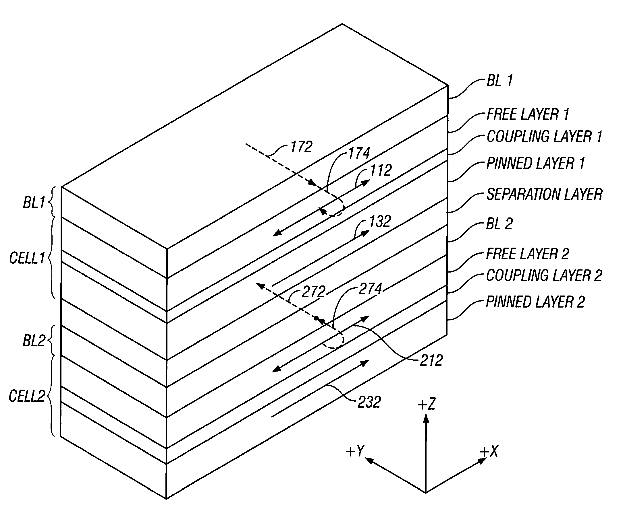
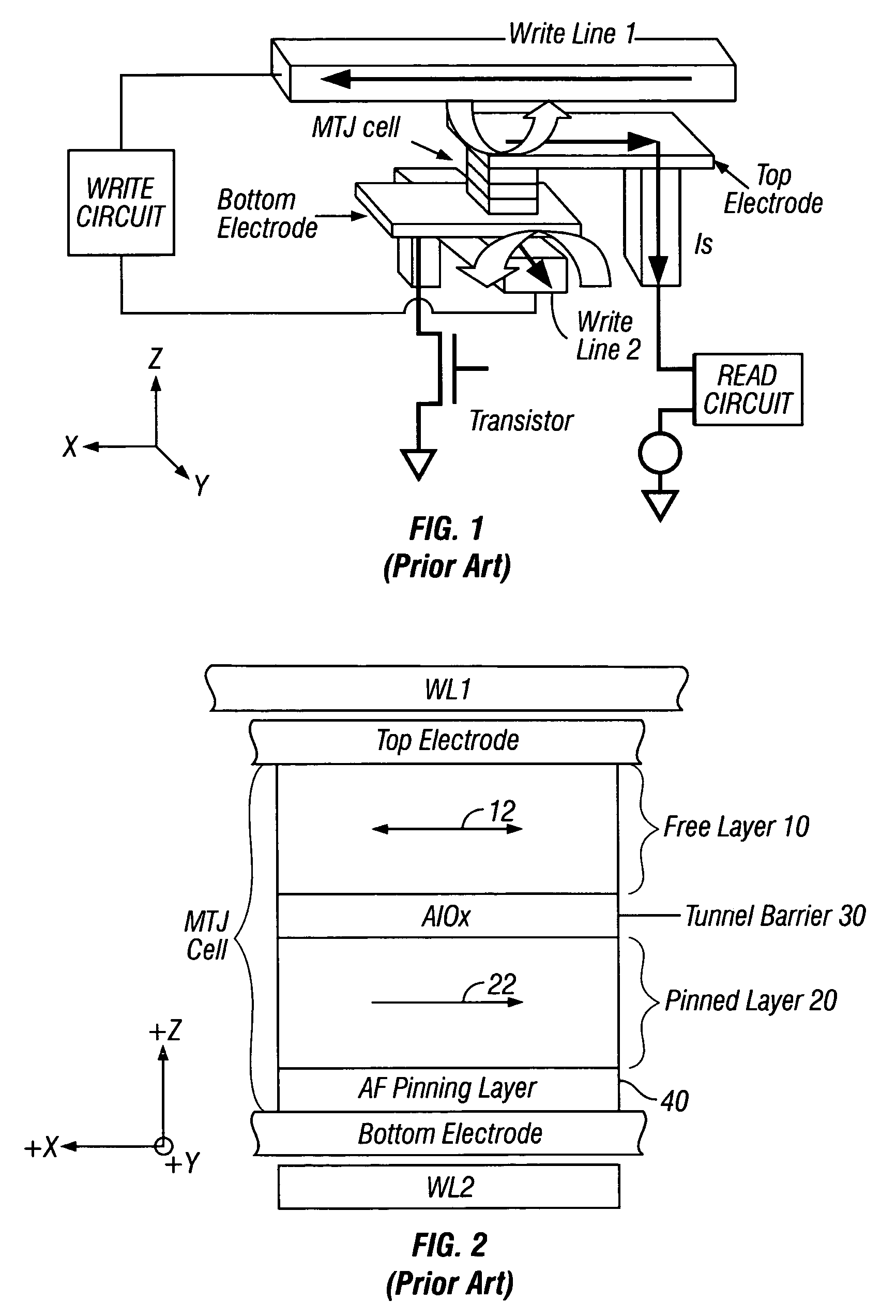
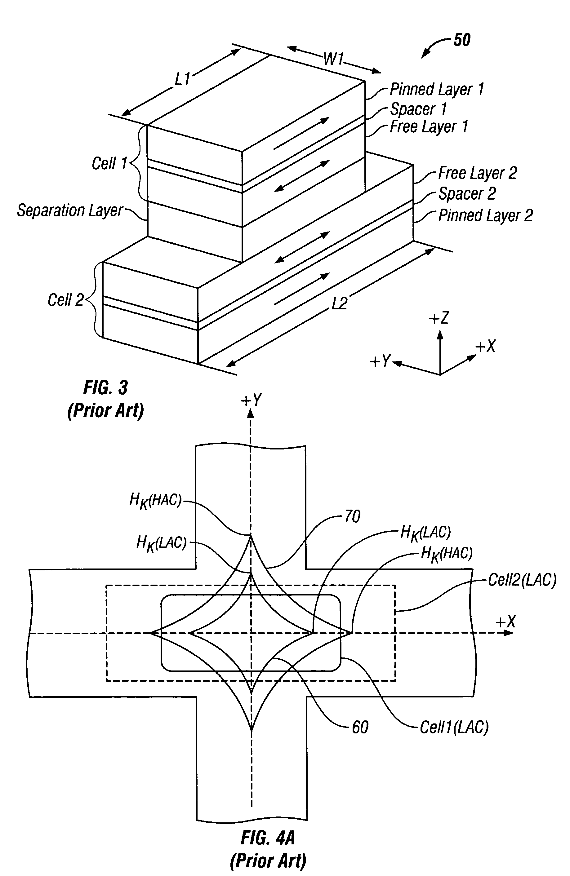
[0026]FIG. 1 is a perspective view of a portion of the prior art a 1T1MTJ MRAM showing a single conventional MTJ memory cell, i.e., a memory cell with two magnetic states representing 0 and 1, with a free ferromagnetic layer whose magnetization direction (or magnetic moment) is switched by application of current through the write lines. The MTJ cell is located in an intersection region between a second write line (WL2) (aligned along the Y axis) and a first write line (WL1) (aligned along the X axis). The write lines are connected to a write circuit that provides the current pulses to perform the writing. Only one MTJ cell and intersection region is depicted in FIG. 1, but in the MRAM there are a plurality of generally parallel second write lines and a plurality of generally parallel first write lines that are orthogonal to the second write lines and overlap to define a plurality of intersection regions. Each intersection region contains an MTJ cell. Each MTJ cell is electr...


PUM


Abstract

A magnetic random access memory (MRAM) has memory stacks arranged in the X-Y plane on the MRAM substrate, with each memory stack having two memory cells stacked along the Z axis and each memory cell having an associated biasing layer. Each biasing layer reduces the switching field of its associated cell by applying a biasing field along the hard-axis of magnetization of the free layer of its associated cell. The free layers in the two cells in each stack have their in-plane easy axes of magnetization aligned parallel to one another. Each biasing layer has its in-plane magnetization direction oriented perpendicular to the easy axis of magnetization (and thus parallel to the hard axis) of the free layer in its associated cell. The hard-axis biasing fields generated by the two biasing layers are in opposite directions.

Description

BACKGROUND OF THE INVENTION[0001]1. Field of the Invention[0002]This invention relates generally to magnetic random access memory (MRAM) and more particularly to MRAM with units or stacks of multiple memory cells for producing more than two logic states.[0003]2. Description of the Related Art[0004]MRAM with magnetic tunnel junction (MTJ) memory cells has been proposed for nonvolatile memory, as described in U.S. Pat. No. 5,640,343 and by Reohr et al., “Memories of Tomorrow”, IEEE CIRCUITS & DEVICES MAGAZINE, September 2002, pp. 17-27. In these devices the MTJ cells are arranged as an array in a single layer (the X-Y plane) on a semiconductor substrate. In one type of architecture, called a 1T1MTJ MRAM (one transistor and one MTJ), each MTJ cell is located between a bit line and a transistor, with the word lines located beneath the MTJ cells. In another type of architecture, called a cross-point (XPC) MRAM, the MTJ cells are located directly between the bit and word lines.[0005]In bo...

Claims


Application Information

Patent Timeline
Patent Type & Authority Patents(United States)
IPC IPC(8): H01L29/82G11C11/50H01L29/94
CPCH01L27/226G11C11/16H10B61/22
Inventor JU, KOCHANCHANG, JEI-WEI
Owner INTELLECTUAL VENTURES HOLDING 81 LLC
Why Eureka
Try Eureka