System and method for enhancing data rates over addressable lighting networks
a technology of addressable lighting and data rate, applied in data switching networks, high-level techniques, digital transmission, etc., can solve the problems of low data rate of dali protocol, reduced effective data rate to about 400 b/s=33.3%1200 b/s, and reduced data rate. effective rate, simple and reliable signaling
- Summary
- Abstract
- Description
- Claims
- Application Information
AI Technical Summary
Benefits of technology
Problems solved by technology
Method used
Image
Examples
first embodiment
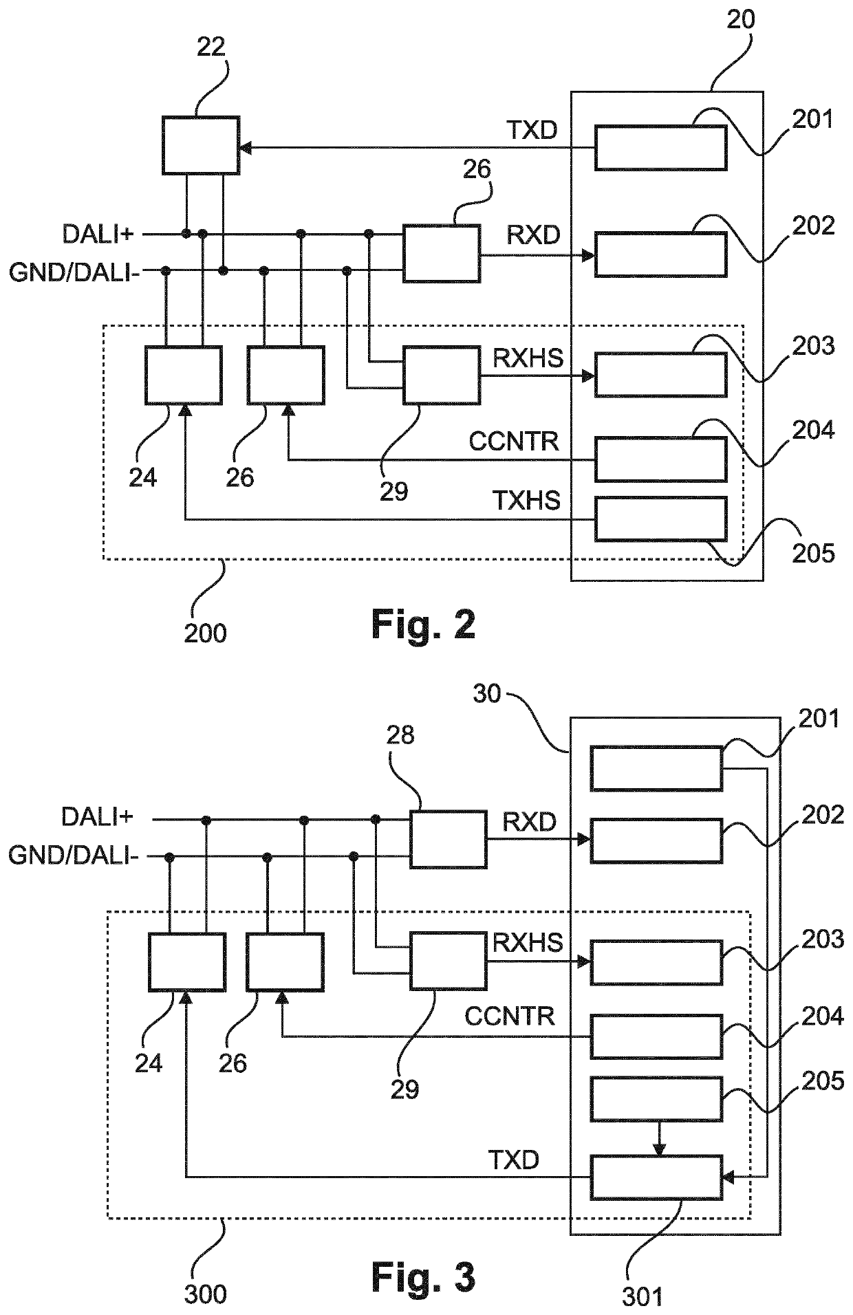
[0028]FIG. 2 shows a schematic block diagram of a proposed communication architecture of a master device to allow high-speed data transfer over DALI bus lines DALI+ and GND / DALI−. The master device comprises a first bus driver 22 and a conventional DALI (high) threshold receiver 28 for low-speed communication. Additionally, a microcontroller 20 is provided as a control unit for implementing a conventional DALI encoder 201 which generates low-rate transmission data TXD supplied to the first bus driver 22. Furthermore, the microcontroller 20 implements a conventional DALI decoder 202 which receives low-rate reception data RXD outputted from the DALI threshold receiver 28.
[0029]In addition, a high-level functional architecture of the proposed communication data-rate enhancement concept according to the first embodiment is shown in FIG. 2, wherein the above conventional DALI architecture is augmented with an additional high-speed communication section 200 comprising additional componen...
third embodiment
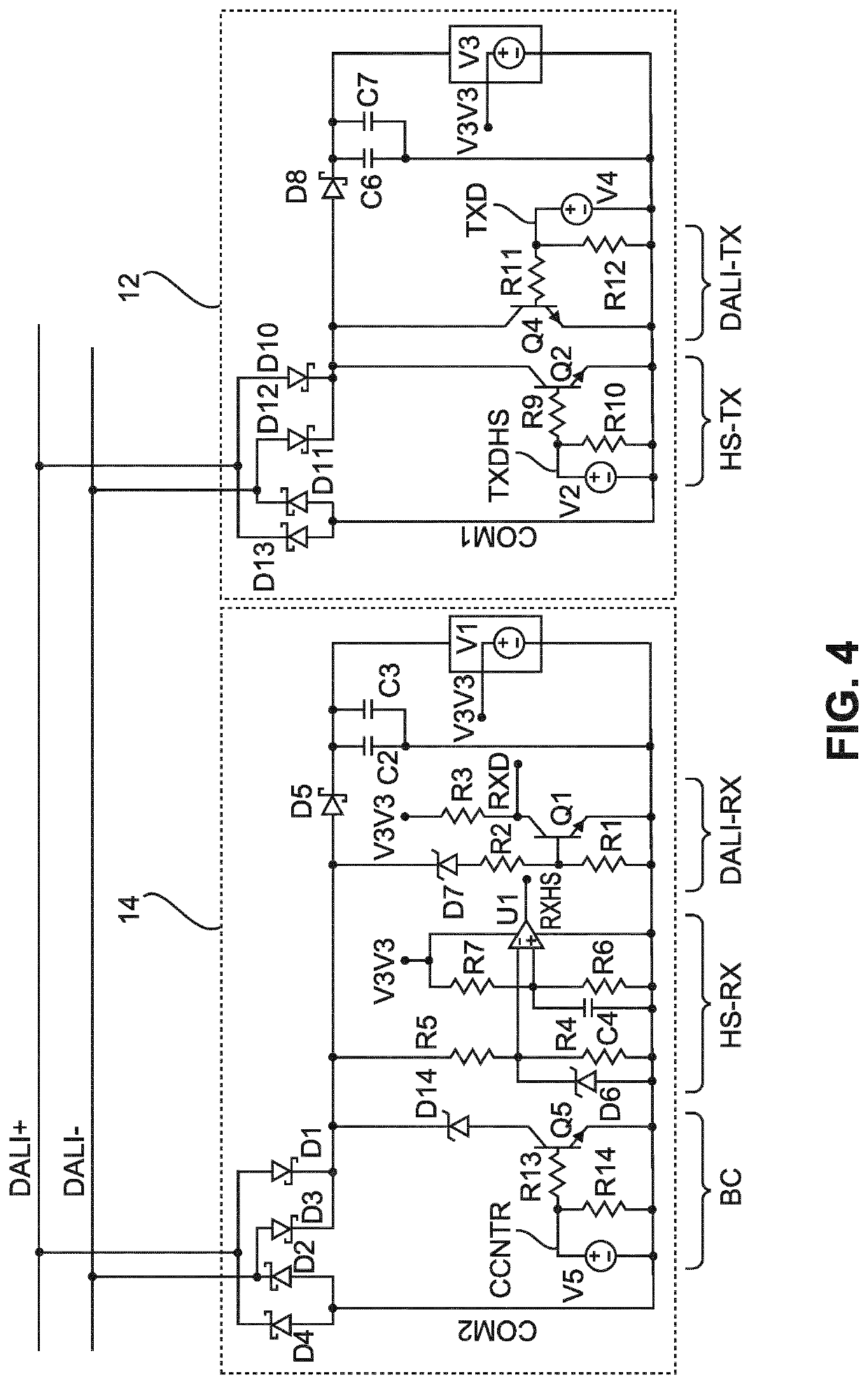
[0034]FIG. 4 shows an exemplary circuit diagram of a bus-type transmission system with selectable data rate according to a
[0035]It is noted that only those circuit components of a master device 14 and a slave devices 12 of the transmission system are shown that are useful for explaining the present invention are shown in FIG. 4. The master and slave devices 14 and 12 are coupled to the DALI bus by respective diode circuits consisting of Schottky diodes D1 to D4 and D10 to D13, respectively. The signal voltages of the master device 14 are referenced to reference potential COM2, while the signal voltages of the slave device 12 are referenced to reference potential COM1.
[0036]In case of the master device 14, the bus clamp circuit (BC) is realized by using a Zener diode D14 as voltage limitation element that restricts the voltage swing of the DALI bus (bus lines DALI+ and DALI−) and a transistor switch Q5 that is controlled by the clamp control signal CCNTR supplied from a voltage sourc...
fourth embodiment
[0048]FIG. 7 shows a schematic flow diagram of a procedure for enhancing data rate on a data bus.
[0049]Respective parts of the procedure can be performed by a controller or processor provided in a master or slave device (e.g. luminaire device of an addressable lighting network) so as to temporary enhance data rates for transmission.
[0050]Initially, in step 701, a slave device notifies a bus master of a need for high-speed communication over the data bus. Then, in step 702, responsive to a receipt of the notification, the bus master activates a bus clamp control so as to limit the signaling voltage on the data bus to a level below the lowest detection threshold of usual low-speed transmission. In the subsequent step 703, the slave node detects the reduced voltage level on the data bus and starts high-speed signaling. In step 704, the detection threshold at the receiving side (master device or addressed other slave device) of the transmission is correspondingly lowered to match the n...
PUM
 Abstract
Description
Claims
Application Information


