Method for die bonding having pick-and-probing feature

a die bonding and feature technology, applied in the direction of semiconductor/solid-state device testing/measurement, measurement devices, instruments, etc., can solve the problems of reducing the yield and productivity of semiconductor packages with higher grades, reducing the productivity of semiconductor packages with lower electrical performance, and reducing the yield of semiconductor packages with higher grades. , to achieve the effect of increasing the productivity of higher graded packages and saving processing tim

Inactive Publication Date: 2009-09-10
POWERTECH TECHNOLOGY
View PDF4 Cites 11 Cited by
  • Summary
  • Abstract
  • Description
  • Claims
  • Application Information

AI Technical Summary

Benefits of technology

[0005]The main purpose of the present invention is to provide a die-bonding method with pick-and-probe features after wafer sawing where die probing and sorting are performed at the same time as picking the dice during die bonding processes without extra sorting steps to reduce processing time. Moreover, higher graded dice and lower graded dice are not mixed together in the same semiconductor packages leading to better productivity of different graded semiconductor packages.
[0006]The second purpose of the present invention is to provide a die-bonding method with pick-and-probe features after wafer sawing to reduce particle contaminations of bonding pads during wafer probing to keep wafers clean.
[0007]The third purpose of the present invention is to provide a die-bonding method with pick-and-probe features after wafer sawing to screen out bad dies during die-bonding processes according to the sorting results to eliminate the risk of probing or sorting errors to maintain higher packaging yields.

Problems solved by technology

Then, individual dice are picked from the die trays or die carrier tapes by a suction nozzle then die bonded to die carriers which is the most time consuming step and greatly reduces the productivity.
If different graded dice are packaged in the same semiconductor package, then the overall operation frequency will base on the die with the lowest grade leading to lower electrical performance of the semiconductor packages.
Moreover, the yield and productivity of semiconductor packages with higher grades are reduced leading to decrease of revenue.

Method used


Image

  • Method for die bonding having pick-and-probing feature
  • Method for die bonding having pick-and-probing feature
  • Method for die bonding having pick-and-probing feature

Examples


Embodiment Construction

[0011]Please refer to the attached drawings, the present invention will be described by means of embodiments below.

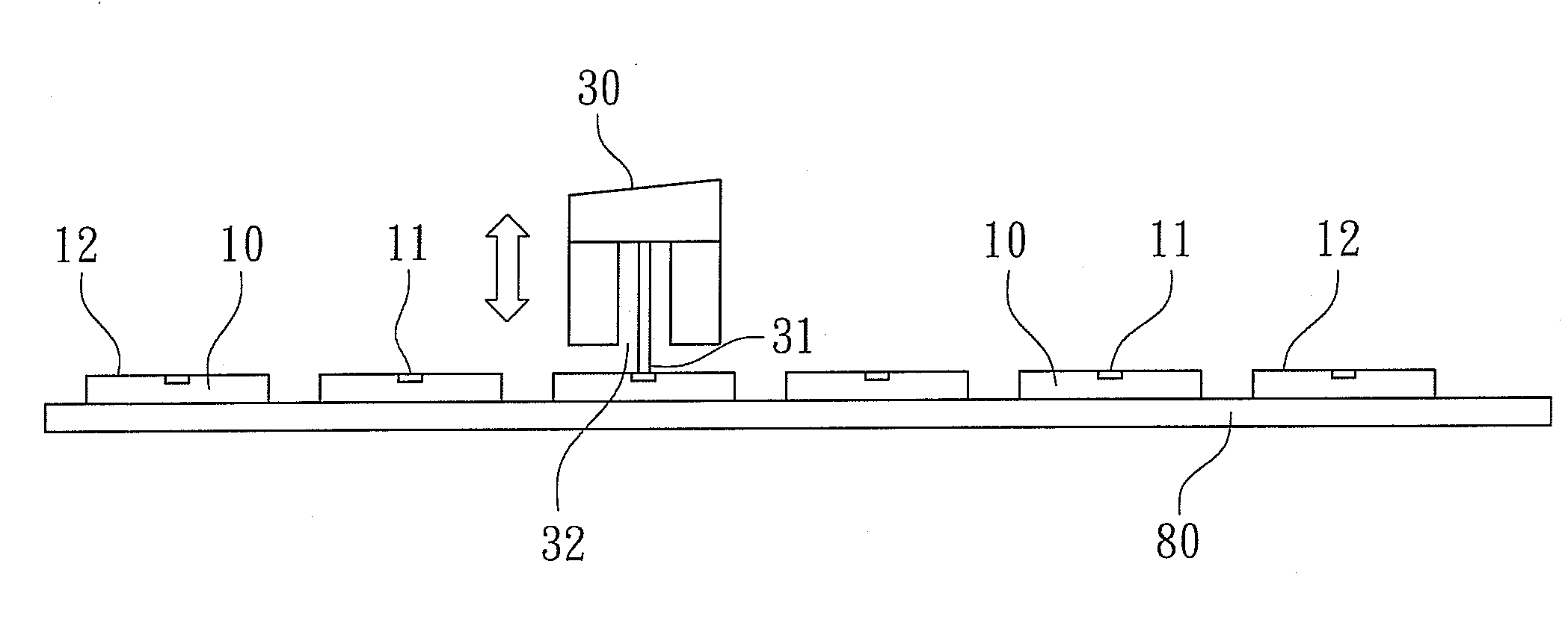
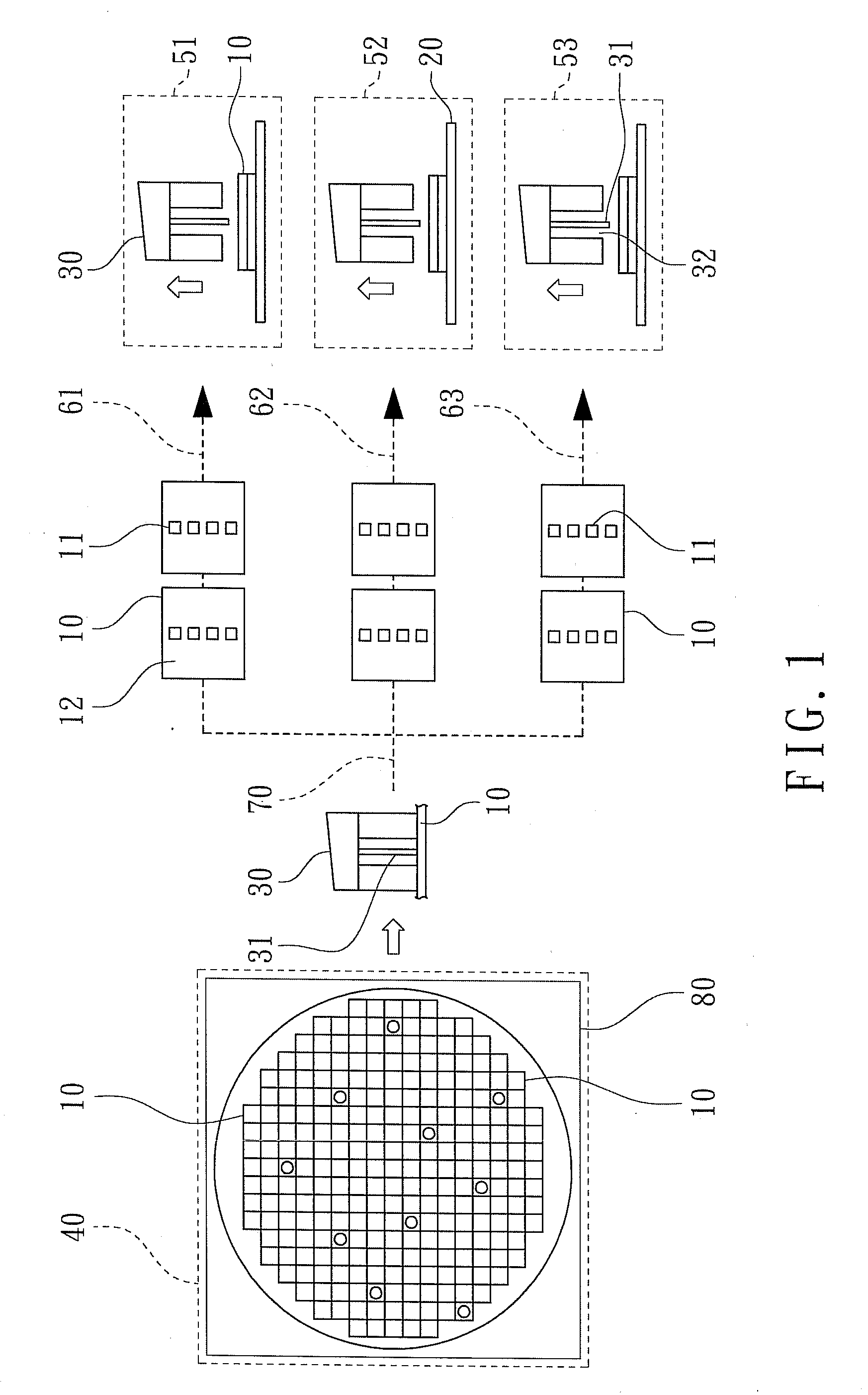
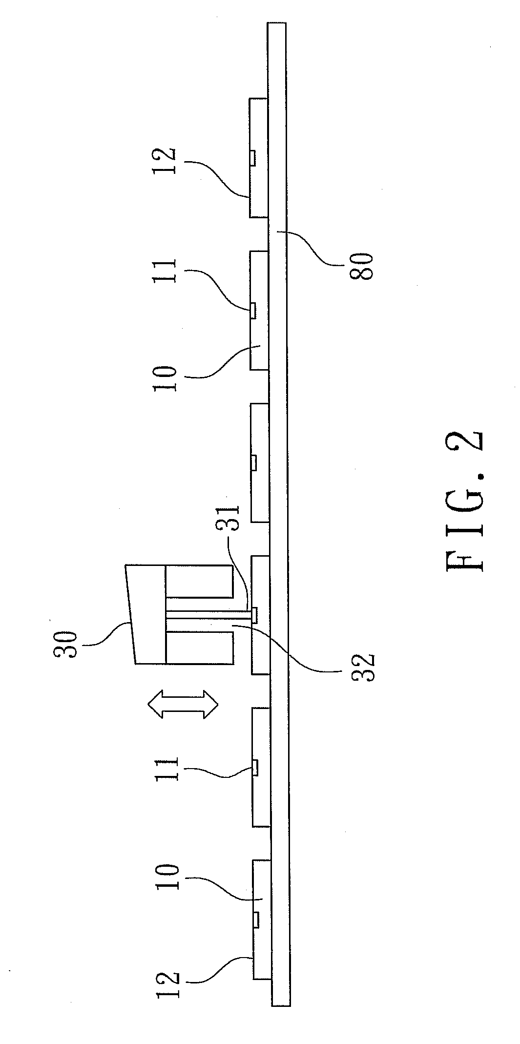
[0012]According to the first embodiment of the present invention, a die-bonding method with pick-and-probe features after wafer sawing comprises the following steps. As shown in FIG. 1, firstly, at least a die 10 is provided where the dice 10 are taken from a singulated wafer. As shown in FIGS. 1 and 2, a plurality of electrical terminals 11 are disposed on the active surface 12 of the die 10. A die-bonding equipment, also known as a die bonder, includes at least a suction nozzle 30, a loading area 40, a plurality of die-bonding areas 51, 52, and 53, and a plurality of sorting paths 61, 62, and 63. Therein, the die-bonding areas 51, 52, and 53 are graded according to a plurality of different die grades, and the sorting paths 61, 62, and 63 is connected from a common moving path 70 connecting the loading area 40 to the corresponding die-bonding areas 51, 52, and 53.

[0013...


PUM


Abstract

Disclosed is a die-bonding method having pick-and-probe features after wafer sawing where at least a die is probed and sorted according to different grades during a pick-and-place step performed after wafer sawing. A suction nozzle having a plurality of probes is utilized to probe the electrical terminals of the die. After picking, the suction nozzle is moved on a common moving path and the picked die is tested through the suction nozzle. The picked-and-probed die is moved and die-bonded to a die carrier loaded in a corresponding one of a plurality of die-bonding areas by moving the Suction nozzle on a chosen sorting path. Therefore, the die is probed and sorted during die-bonding processes. Higher graded dice at a same level are assembled on a same die carrier to form a higher graded semiconductor package.

Description

FIELD OF THE INVENTION[0001]The present invention relates to fabrication technologies of semiconductor devices about a die-bonding method after wafer sawing, especially to a die-bonding method with pick-and-probe features after wafer sawing.BACKGROUND OF THE INVENTION[0002]In semiconductor front-end fabrication, the process flow is IC design, wafer fabrication, wafer probing, and wafer sawing. After wafer probing and wafer sawing processes, individual IC dice are formed for semiconductor packaging.[0003]Whether the electrical performance and characteristics of each IC die have met the design specifications are confirmed by testers and probe cards to probe every die on a wafer. The probes of a probe card mounted on the tester head of a tester keep in contact with the bonding pads of a die to test its electrical characteristics and then failed dice will be marked. After wafer sawing, a wafer is diced into a plurality of individual dice where some of the dice with marks are scrapped wi...

Claims


Application Information

Patent Timeline
Patent Type & Authority Applications(United States)
IPC IPC(8): H01L21/66
CPCH01L21/67271H01L21/67144
Inventor FANG, LI-CHIHFAN, WEN-JENGLIN, NAN-CHUN
Owner POWERTECH TECHNOLOGY
Why Eureka
Try Eureka