Apparatus and method for etching the surface of a semiconductor substrate

a technology of etching bath and semiconductor substrate, which is applied in the direction of electrical apparatus, semiconductor devices, photovoltaic energy generation, etc., can solve the problems of affecting the etching process

Inactive Publication Date: 2009-09-10
GRACO FLUID HANDLING H INC
View PDF19 Cites 15 Cited by
  • Summary
  • Abstract
  • Description
  • Claims
  • Application Information

AI Technical Summary

Problems solved by technology

The use of both wet etching and dry etching is a drawback
The use of multiple tanks creates unneeded complexity.
The Jeong patent creates turbulent flow in the processing area and generates bubbles that can hinder the etching process.
The described method does not produce a uniform flow rate or remove bubbles.
There are a number of drawbacks involved with the above-described methods and devices.
In such prior art devices it is difficult to obtain a uniform flow rate across the semiconductor surface.

Method used


Image

  • Apparatus and method for etching the surface of a semiconductor substrate
  • Apparatus and method for etching the surface of a semiconductor substrate
  • Apparatus and method for etching the surface of a semiconductor substrate

Examples


Embodiment Construction

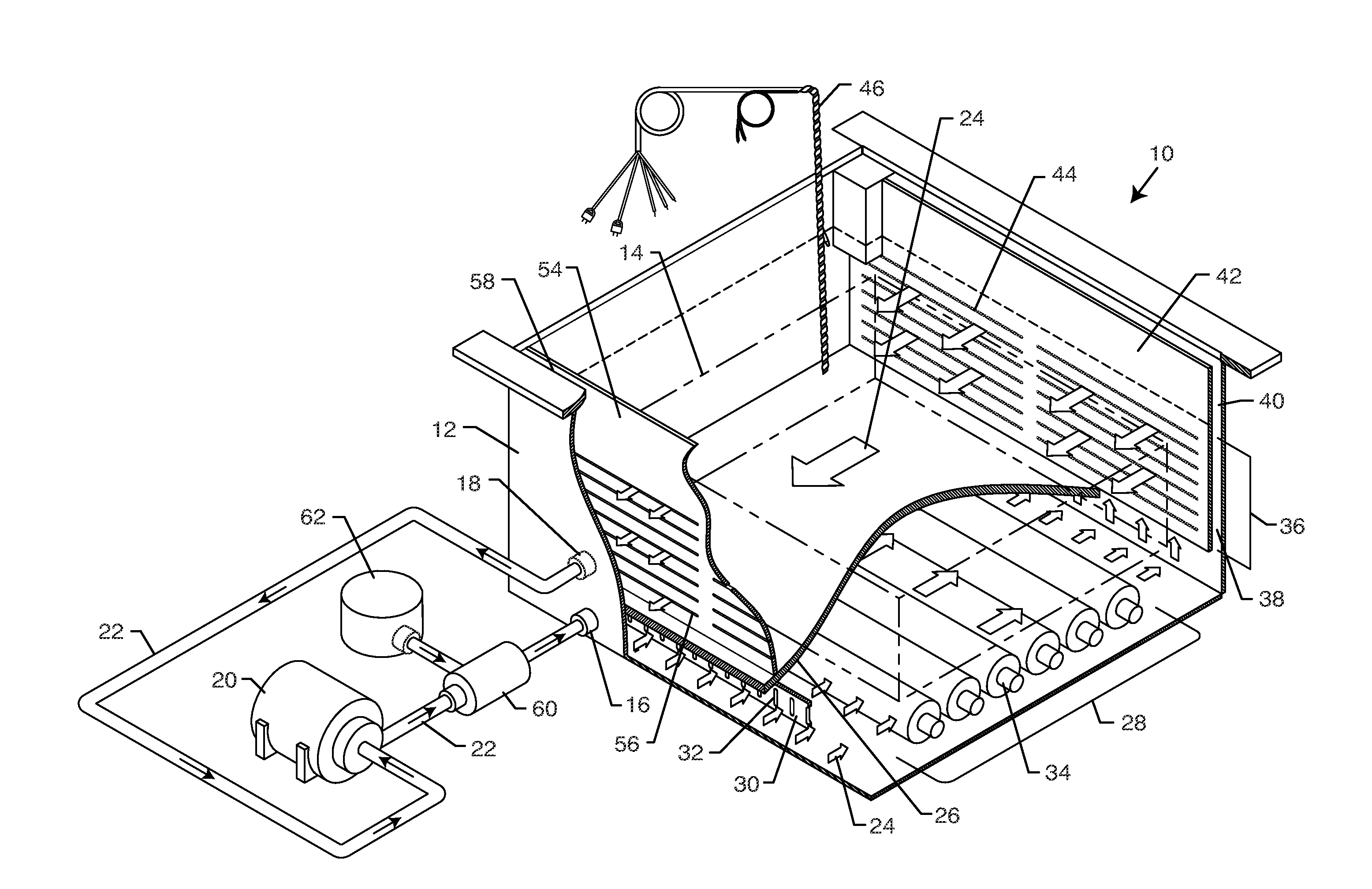
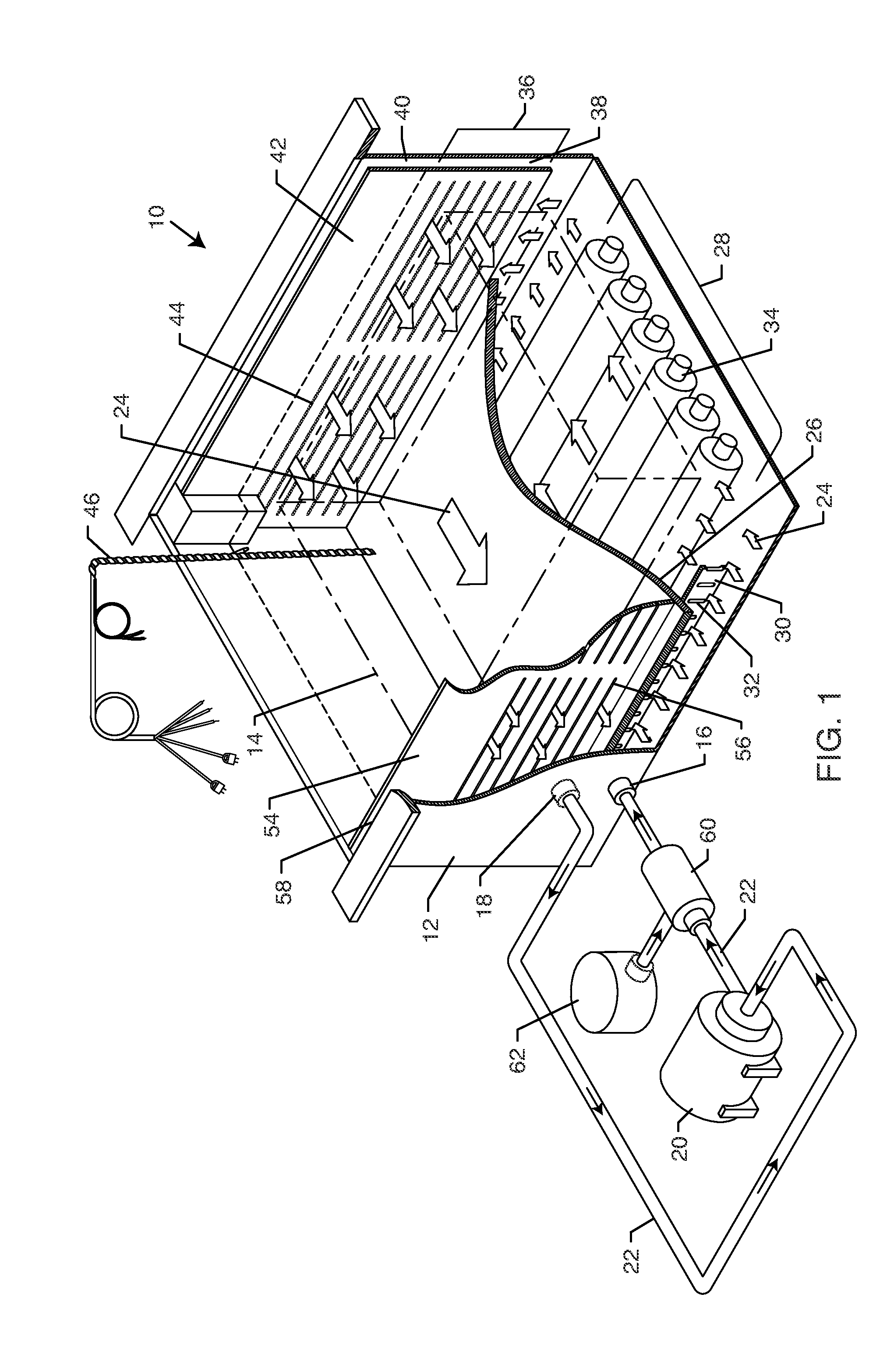
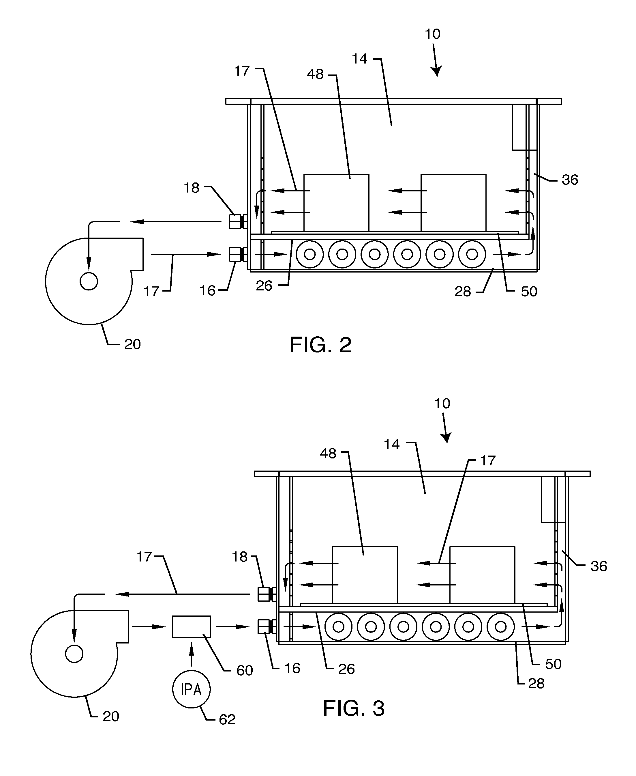
[0033]The present invention relates to a process and apparatus for etching the surfaces of semiconductor substrates, primarily silicon. In particular, the present invention relates to a recirculating texturing tank and the process employed therein. The inventive texturing tank shortens the processing time required to etch the surfaces of semiconductor substrates by creating a more uniform flow across the surface of the substrates to be etched. In current methods, manufacturers use either a static tank in which the substrates see no flow, or an overflow tank in which some substrates see a greater flow than others. By introducing flow in a controlled, uniform manner the substrates are etched quicker and more consistently. Such a system facilitates mass production utilization because greater production can be achieved in a shorter amount of time with more uniform quality. These flow characteristics also act to remove and eliminate bubbles and other particulates from the surfaces of the...


PUM

PropertyMeasurementUnit
concentrationaaaaaaaaaa
areaaaaaaaaaaa
temperatureaaaaaaaaaa

Abstract

A process for etching the surfaces of semiconductor substrates utilizes a texturing tank which introduces a process fluid through a circulating system. The process fluid is heated to a desired temperature and maintained at a desired concentration prior to entering a processing area where laminar flow is produced to more quickly and uniformly roughen the surface of semiconductor substrates. The texturing tank permits removal of bubbles and eliminates temperature stratification in the processing area.

Description

FIELD OF THE INVENTION[0001]The present invention relates to an etching bath for etching the surfaces of semiconductor substrates, primarily silicon. In particular, the present invention relates to a texturing tank and a process used therein in the fabrication of a non-reflective surface on silicon solar cells.BACKGROUND OF THE INVENTION[0002]Solar cells are devices that convert light energy incident to its surface into electrical energy. Past efforts and ongoing research have led to improved efficiency by finding methods to convert more of the incident light energy into electrical energy. Several such improvements involve processes for roughening or texturing the surface of the solar cell substrate in order to reduce its reflective quality and therefore absorb more incident light for conversion. The texturing procedures improve the silicon solar efficiency by forming minute projections and recesses on the surface so that incident light is absorbed rather than reflected.[0003]Variou...

Claims


Application Information

Patent Timeline
Patent Type & Authority Applications(United States)
IPC IPC(8): H01L21/306
CPCH01L21/67086Y02E10/50H01L31/02363
Inventor RAMIREZ, JORGECASTANEDA, HECTOR JOELTIONGCO, MELISSA A.
Owner GRACO FLUID HANDLING H INC
Why Eureka
Try Eureka