Insulating circuit board and insulating circuit board having cooling sink
- Summary
- Abstract
- Description
- Claims
- Application Information
AI Technical Summary
Benefits of technology
Problems solved by technology
Method used
Image

Examples
first verification experiment
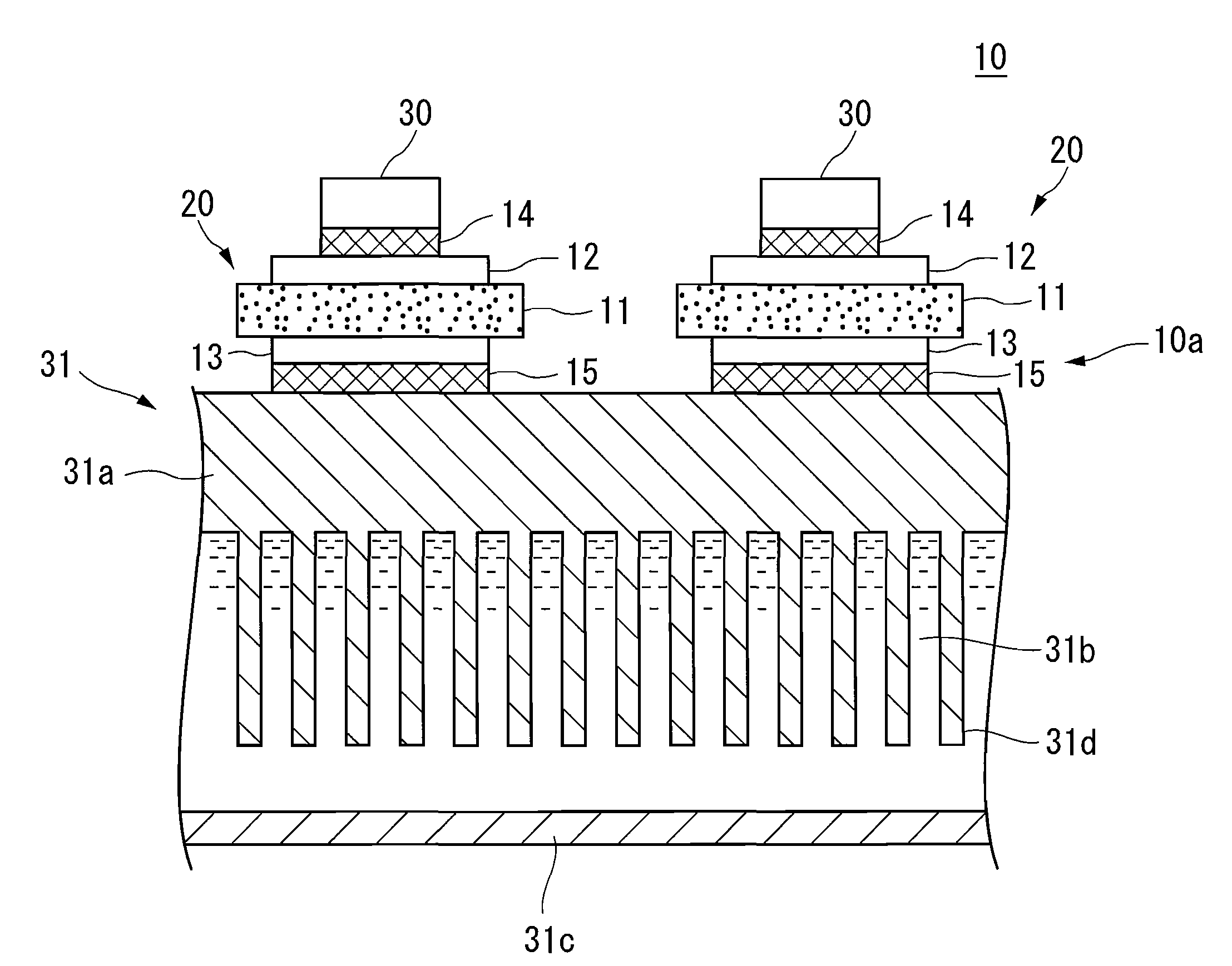
[0062]Here, among the above effects, the effect that cracks can be prevented from being generated and growing in the first solder layer 14 and the second solder layer 15 by forming the circuit board 12 from an Al alloy having a purity of 99.98% or more or pure Al and by forming the metal plate 13 from an Al alloy having a purity of 98.00% or more and 99.90% or less was verified by an experiment (hereinafter referred to as “first verification experiment”).
[0063]The following configuration was adopted as an insulating circuit board having a cooling sink provided for this experiment.
[0064]The insulating plate 11 was formed from a material containing AlN as its main component, and the length, width, and thickness thereof were 50 mm, 50 mm, and 0.635 mm, respectively. The circuit board 12 was formed from an Al alloy, and the length, width, and thickness thereof were 48 mm, 48 mm, and 0.4 mm, respectively. The metal plate 13 was formed from an Al alloy, and the length, width, and thicknes...
second verification experiment
[0072]Next, the effect that the stresses generated in the first solder layer 14 and the second solder layer 15 due to a heat cycle could be relieved by setting the thickness of the metal plate 13 and the thickness of the circuit board 12 to the above ranges was verified by an experiment (hereinafter referred to as “second verification experiment”).
[0073]As power modules provided for this experiment, there were adopted 49 types of power modules having the same configurations as the power modules adopted in the first verification experiment, except that the circuit board 12 was formed from an Al alloy having a purity of 99.99%, the metal plate 13 was formed from an Al alloy having a purity of 99.50%, and the thicknesses of the circuit board 12 and the metal plate 13 varied within a range from 0.2 mm to 1.5 mm. Hereinafter, configurations in which the thickness (a) of the circuit board 12 was 0.2 mm or more and 0.8 mm or less, the thickness (b) of the metal plate 13 was 0.6 mm or more ...
third verification experiment
[0077]Next, the verification experiment to determine that cracking could be prevented from being caused in the second solder layer 15 by setting the Young's modulus, 0.2% proof stress, and tensile strength of the second solder layer 15 to the above magnitudes, respectively, was implemented.
[0078]As power modules provided for this experiment, there were prepared 10 types of power modules having the same configurations as the power modules adopted in the first verification experiment, except that the circuit board 12 was formed from an Al alloy having a purity of 99.99%, the metal plate 13 was formed from an Al alloy having a purity of 99.50%, and the material of the second solder layer 15 varied.
[0079]Hereinafter, cases where the material of the second solder layer 15 was a solder including a ternary or more multi-component alloy containing 85 wt % or more of Sn, 0.5 wt % or more of Ag, and 0.1 wt % or more of Cu are referred to as third examples, and configurations other than the th...
PUM
 Abstract
Description
Claims
Application Information
 - Generate Ideas
- Intellectual Property
- Life Sciences
- Materials
- Tech Scout
- Unparalleled Data Quality
- Higher Quality Content
- 60% Fewer Hallucinations
Browse by: Latest US Patents, China's latest patents, Technical Efficacy Thesaurus, Application Domain, Technology Topic, Popular Technical Reports.
© 2025 PatSnap. All rights reserved.Legal|Privacy policy|Modern Slavery Act Transparency Statement|Sitemap|About US| Contact US: help@patsnap.com