LED package and method of manufacturing the same

a technology of light-emitting diodes and led packages, which is applied in the direction of semiconductor/solid-state device manufacturing, electrical equipment, semiconductor devices, etc., can solve the problems of increasing manufacturing costs, difficulty in filling dispensers d, and increasing color coordinate variation, so as to reduce the variation of color coordinates

Inactive Publication Date: 2009-09-17
SAMSUNG LED CO LTD
View PDF3 Cites 22 Cited by
  • Summary
  • Abstract
  • Description
  • Claims
  • Application Information

AI Technical Summary

Benefits of technology

[0015]An aspect of the present invention provides an LED package and a method of manufacturing the same that can reduce a variation of color coordinates of mass-produced LED packages, and manufacture LED packages of varying thickness by using one lead frame.

Problems solved by technology

Further, it is also difficult for the dispenser D to fill each of the plurality of buckets B with the exact same amount of filler (since the bucket B is filled with a very small amount of filler).
Even when LED packages emit light of the same color, color coordinates become slightly different from each other, which results in an increase in the variation of the color coordinates.
Further, since lead frames need to be designed and manufactured according to the varying thickness of the LED packages, manufacturing costs increase.

Method used


Image

  • LED package and method of manufacturing the same
  • LED package and method of manufacturing the same
  • LED package and method of manufacturing the same

Examples


Embodiment Construction

[0032]An LED package and a method of manufacturing the same according to exemplary embodiments of the present invention will now be described in detail with reference to the accompanying drawings.

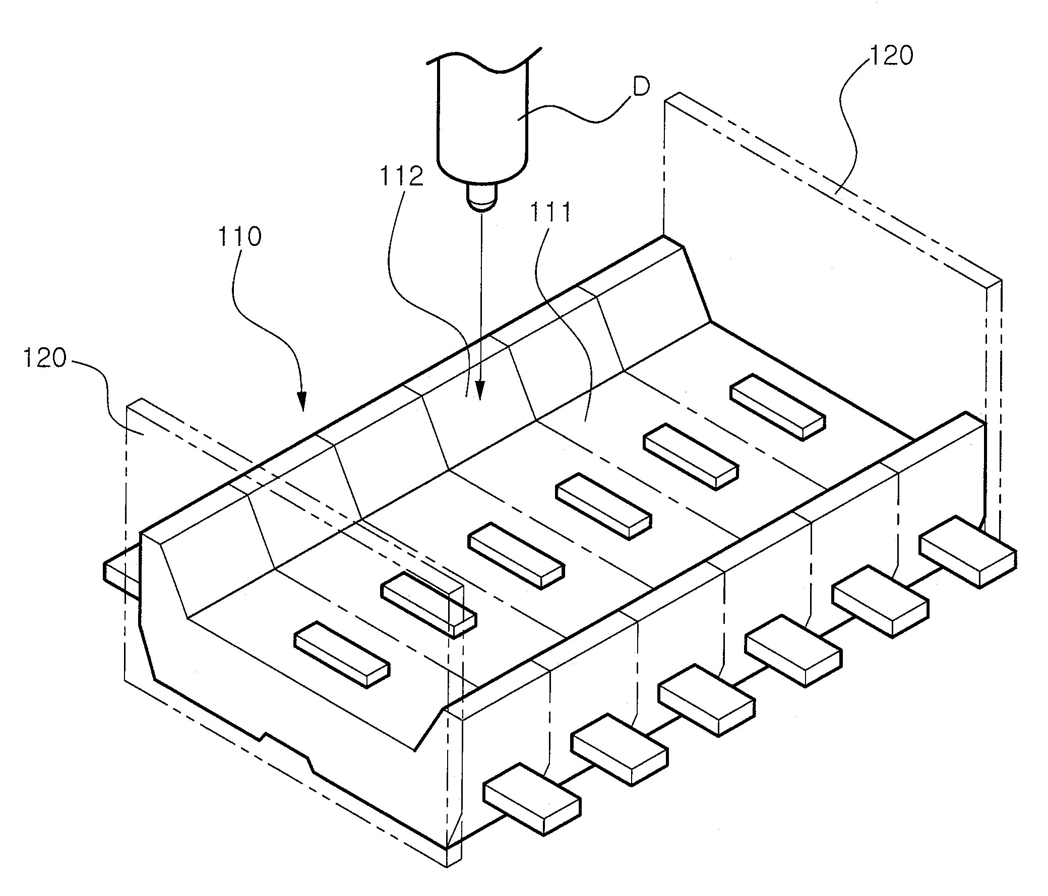
[0033]First, an LED package according to an exemplary embodiment of the invention will be described with reference to FIG. 3. FIG. 3 is a perspective view illustrating the LED package according to the embodiment of the invention.

[0034]As shown in FIG. 3, an LED package 10 according to an exemplary embodiment of the invention includes a base part 11, a filling part 12, and an electrode part 13.

[0035]Partition wall portions 11b are formed at both sides of the base part 11, and a mounting portion 11a is provided between the partition wall portions 11b.

[0036]An LED chip (not shown) is connected to the mounting portion 11a by bonding (including at least one of die bonding and wire bonding). As the filling part 12 fills in the mounting portion 11a, the LED chip is buried in the filling part 12. ...


PUM


Abstract

The present invention relates to light emitting diode (LED) packages and methods of manufacturing the same, and more particularly, to an LED package and a method of manufacturing the same that can reduce a variation of color coordinates of mass-produced LED packages.

Description

CROSS-REFERENCE TO RELATED APPLICATIONS[0001]This application claims the priority of Korean Patent Application No. 2008-0024329 filed on Mar. 17, 2008, in the Korean Intellectual Property Office, the disclosure of which is incorporated herein by reference.BACKGROUND OF THE INVENTION[0002]1. Field of the Invention[0003]The present invention relates to light emitting diode (LED) packages and methods of manufacturing the same, and more particularly, to an LED package and a method of manufacturing the same that can reduce a variation of color coordinates of mass-produced LED packages.[0004]2. Description of the Related Art[0005]In general, light emitting diode (hereinafter, simply referred to as an “LED”) packages that include LEDs to generate light emission according to electrical signals are widely used in a wide variety of electronic products including mobile communication terminals, such as personal cellular phones, and PDAs.[0006]A lead frame is used, a filler, obtained by mixing p...

Claims


Application Information

Patent Timeline
Patent Type & Authority Applications(United States)
IPC IPC(8): H01L33/00H01L21/00H01L33/48H01L33/60
CPCH01L33/60H01L33/486H01L2224/48091H01L2924/00014
Inventor JOUNG, IL KWEON
Owner SAMSUNG LED CO LTD
Why Eureka
Try Eureka