
Light emitting element

a technology of light-emitting elements and light-emitting elements, which is applied in the direction of basic electric elements, electrical equipment, and semiconductor devices, etc., can solve the problems of blue ring, irregular distribution of white light, and certain problems, so as to reduce color variation

Active Publication Date: 2012-03-08
SEOUL VIOSYS CO LTD
View PDF43 Cites 6 Cited by
  • Summary
  • Abstract
  • Description
  • Claims
  • Application Information

AI Technical Summary

Benefits of technology

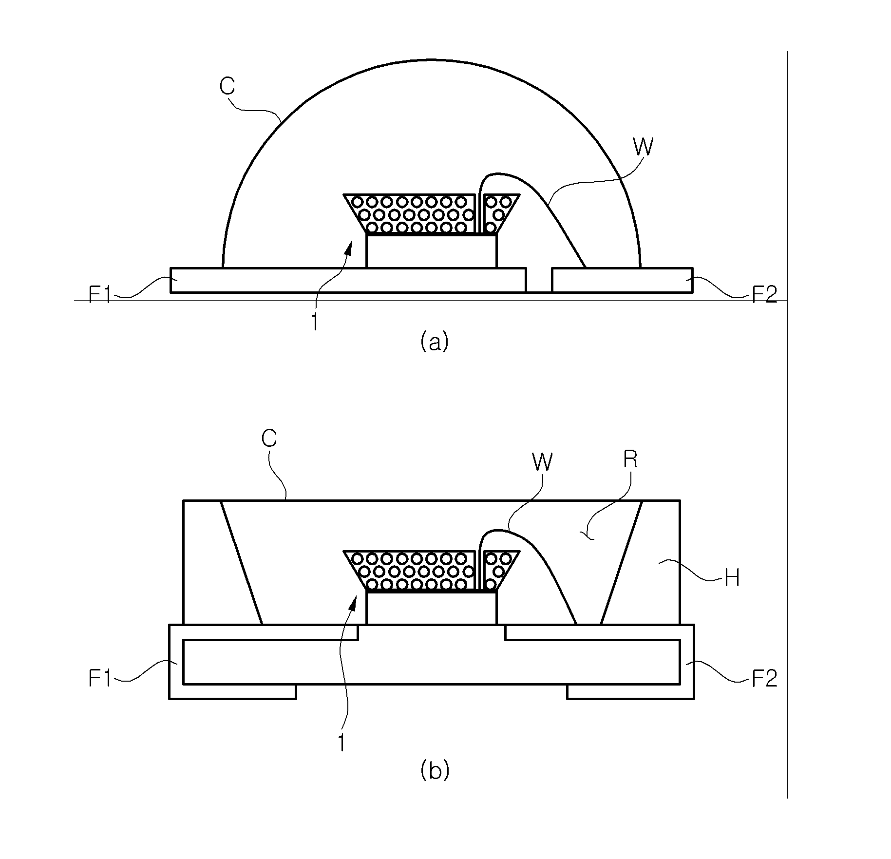
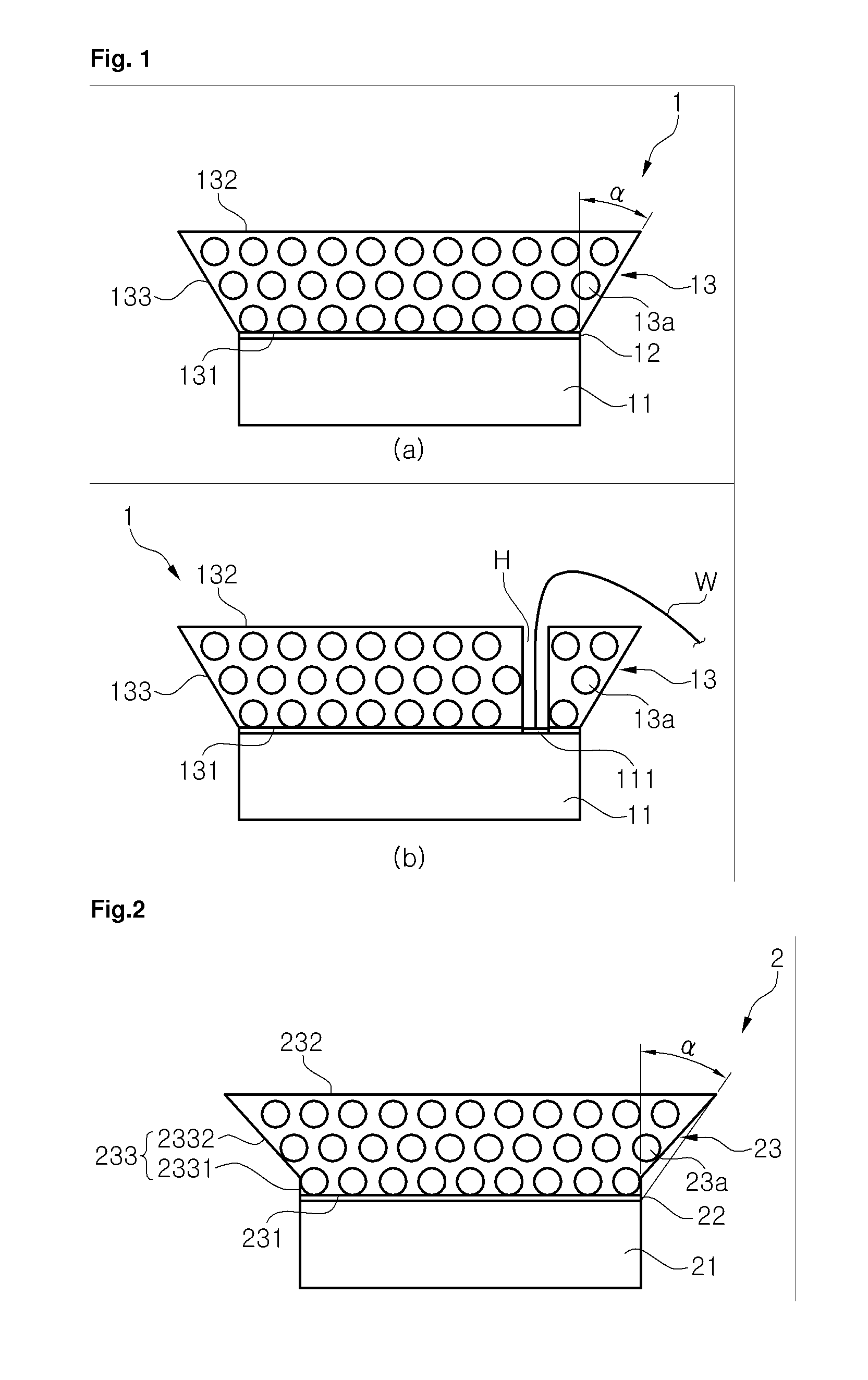
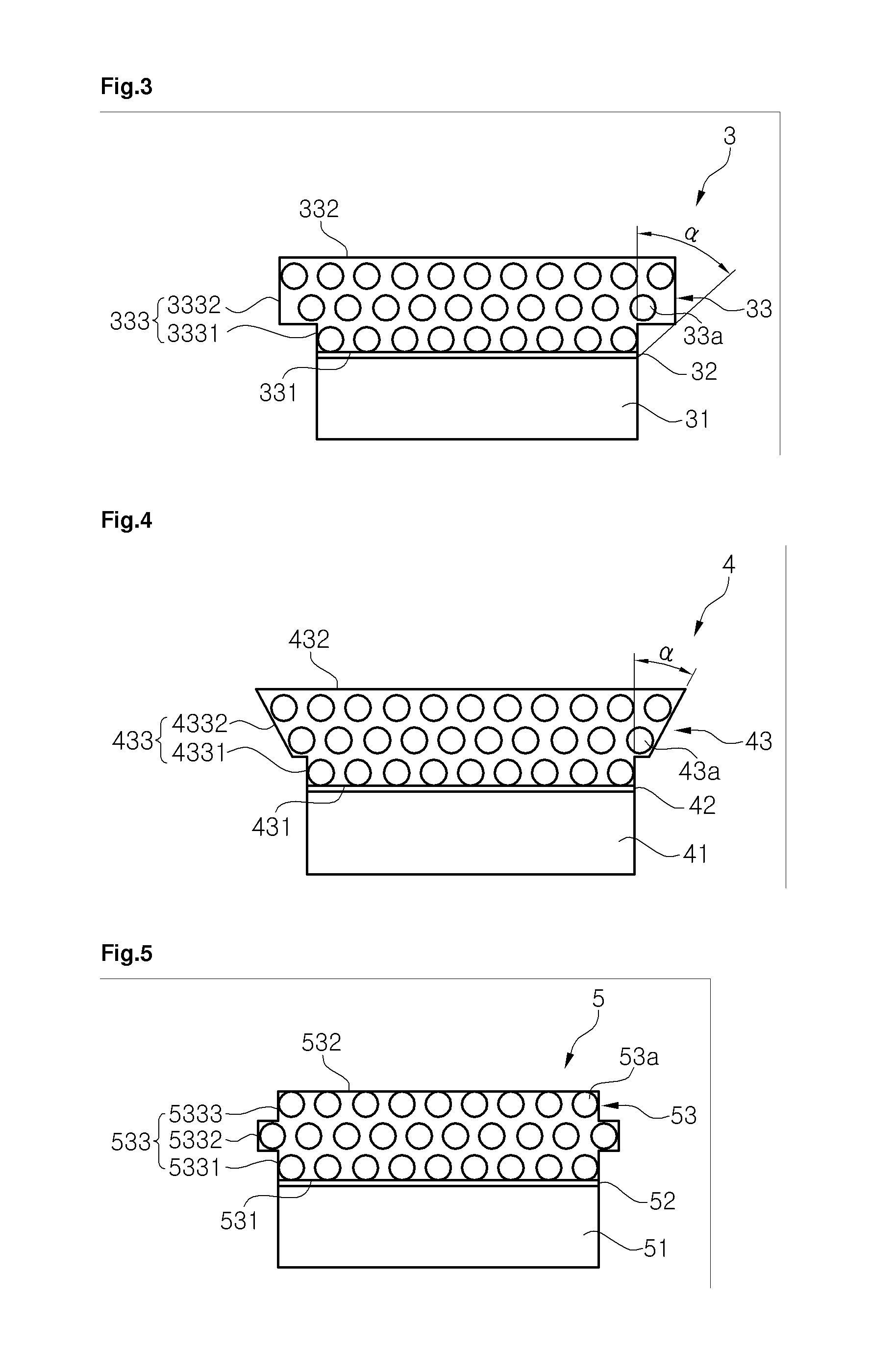
[0008]Exemplary embodiments of the present invention provide a light emitting element including a wavelength-converting layer arranged on an LED chip. The wavelength-converting layer may reduce a color variation generated between a vertical surface and a side of the LED chip. The wavelength-converting layer may be arranged on an upper surface of the LED chip and uniformly color-convert the light emitted from the LED chip.

Problems solved by technology

However, if the area of the wavelength-converting sheet is smaller or greater than the area of the upper surface of the LED chip, certain problems may occur.
In a case where the area of the surface of the wavelength-converting sheet contacting the upper surface of the LED chip is smaller than the area of the upper surface of the LED chip, the light output from the LED chip may be partially emitted without wavelength conversion, which results in irregular distribution of white light and occurrence of a blue ring.

Method used


Image

  • Light emitting element
  • Light emitting element
  • Light emitting element

Examples


Embodiment Construction

[0017]Hereinafter, exemplary embodiments of the present invention will be described in detail with reference to the accompanying drawings. The following embodiments are provided only for illustrative purposes so that those skilled in the art can fully understand the spirit of the present invention. Therefore, the present invention is not limited to the following embodiments but may be implemented in other forms. In the drawings, the widths, lengths, thicknesses and the like of elements may be exaggerated for convenience of illustration. Like reference numerals indicate like elements throughout the specification and drawings.

[0018]It will be understood that when an element or layer is referred to as being “on” or “connected to” another element or layer, it can be directly on or directly connected to the other element or layer, or intervening elements or layers may be present. In contrast, when an element is referred to as being “directly on” or “directly connected to” another element...


PUM


Abstract

The present invention provides a light emitting element, which includes a light emitting diode (LED) chip and a wavelength-converting layer arranged on a surface of the LED chip, the wavelength-converting layer to convert a wavelength of light emitted from the LED chip, wherein at least a portion of the wavelength-converting layer has a width greater than the width of the surface of the LED chip.

Description

[0001]This application claims priority from and the benefit of Korean Patent Application No. 2010-0086802, filed on Sep. 6, 2010, which is hereby incorporated by reference for all purposes as if fully set forth herein.BACKGROUND OF THE INVENTION[0002]1. Field of the Invention[0003]The present invention relates to a light emitting element, and more particularly, to a light emitting element including a wavelength-converting layer arranged on an upper surface of a light emitting diode (LED) chip. The wavelength-converting layer may reduce a color variation generated between a vertical surface and a side of the LED chip.[0004]2. Discussion of the Background[0005]Methods for realizing a white light source using LEDs may be classified into: a method for combining an LED chip emitting blue light and a yellow phosphor; a method for combining an LED chip emitting blue light, an LED chip emitting red light and an LED chip emitting green light without any combination of phosphors; and a method...

Claims


Application Information

Patent Timeline
Patent Type & Authority Applications(United States)
IPC IPC(8): H01L33/50
CPCH01L33/54H01L33/505H01L2924/181H01L2224/48091H01L2924/00014H01L2924/00012H01L2933/0041
Inventor KIM, EU GENE
Owner SEOUL VIOSYS CO LTD
Learn More