Semiconductor device

a technology of semiconductor devices and devices, applied in semiconductor devices, semiconductor/solid-state device details, electrical apparatus, etc., can solve problems such as malfunction of semiconductor devices

Inactive Publication Date: 2009-09-17
RENESAS ELECTRONICS CORP
View PDF3 Cites 5 Cited by
  • Summary
  • Abstract
  • Description
  • Claims
  • Application Information

AI Technical Summary

Benefits of technology

[0008]The present invention has been made in view of the above-mentioned problem, and therefore has an object to provide a semiconductor device which may prevent malfunction thereof under the influence of an infrared laser applied to an encapsulating resin when marking is made.
[0009]A semiconductor device according to the present invention includes: a package substrate; a connecting portion provided on the package substrate; a semiconductor substrate having a main surface and a surface opposite to the main surface, the main surface having connecting terminals formed so as to correspond to the connecting portion and electrically connected to the connecting portion, and the surface opposite to the main surface having a thin film formed t

Problems solved by technology

Thus, there arises a problem in that the semiconductor device malfunctions und

Method used


Image

  • Semiconductor device
  • Semiconductor device
  • Semiconductor device

Examples


Embodiment Construction

[0025]The invention will be now described herein with reference to illustrative embodiments. Those skilled in the art will recognize that many alternative embodiments can be accomplished using the teachings of the present invention and that the invention is not limited to the embodiments illustrated for explanatory purposes.

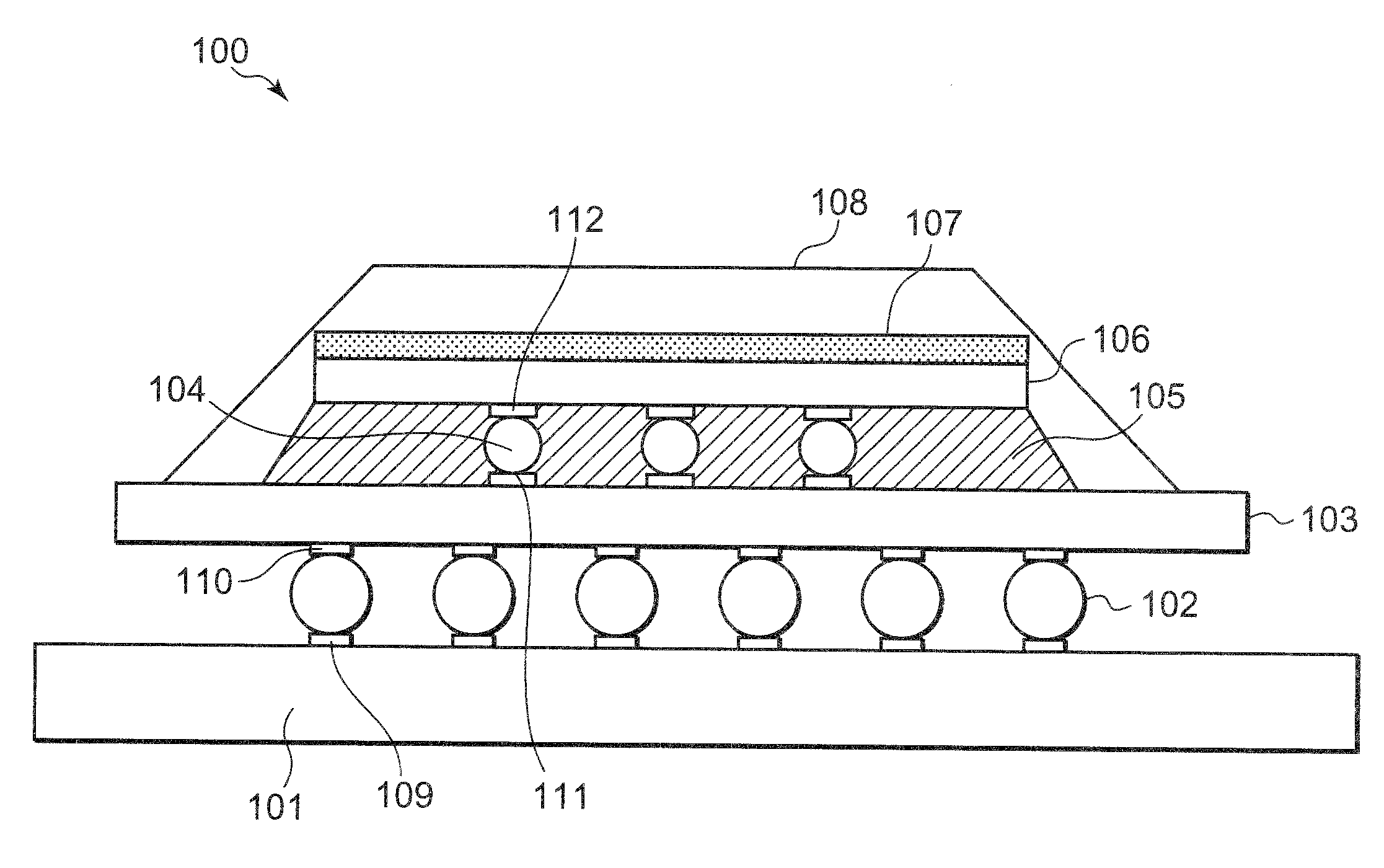
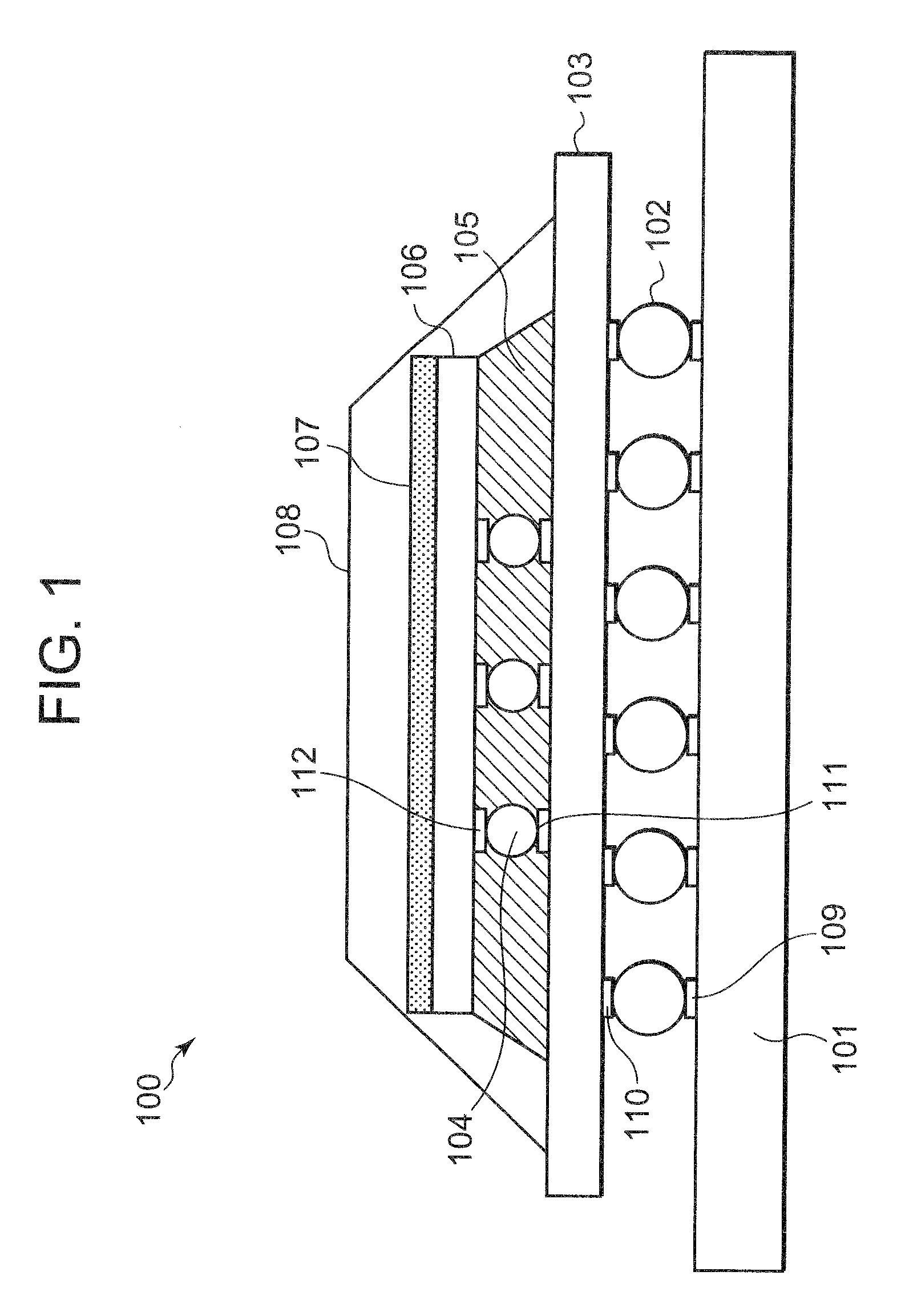
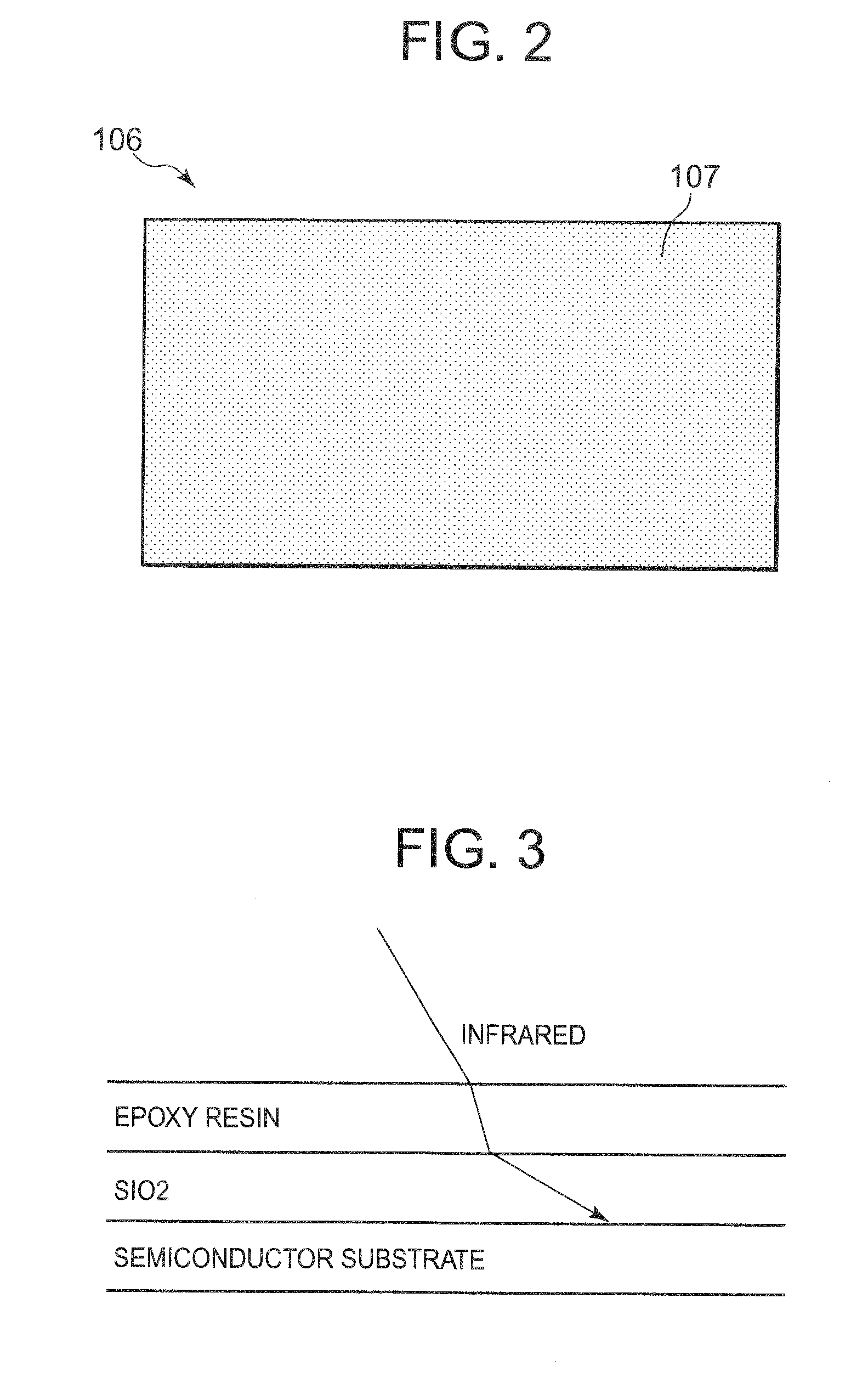
[0026]The best mode for carrying out the present invention is described in the following with reference to the attached drawings. FIG. 1 illustrates a semiconductor device 100 according to an embodiment of the present invention. The semiconductor device 100 is mounted on a mounting substrate 101. A plurality of solder balls 102 provided on the mounting substrate 101 so as to be spaced apart from one another electrically connect the mounting substrate 101 and a package substrate 103 via connecting terminals 109 provided on an upper surface of the mounting substrate 101 and connecting terminals 110 provided on a lower surface of the package substrate 103. The packa...


PUM


Abstract

In recent years, as electronic equipment becomes thinner, an area for mounting a semiconductor device used in the electronic equipment is required to be smaller, and a thickness of an encapsulating resin for encapsulating a semiconductor substrate having a circuit formed thereon and the like also becomes smaller. The encapsulating resin is marked with a product number, a manufacturer name, or the like. There arises a problem in that, in the marking, an infrared laser beam applied to the encapsulating resin passes through the encapsulating resin, generates heat in the semiconductor substrate, and destructs the formed circuit. By providing a thin film for refracting the infrared laser beam on a rear surface of the semiconductor substrate, the optical path of the infrared laser beam is made longer to reduce heat generated in the semiconductor substrate.

Description

BACKGROUND OF THE INVENTION[0001]1. Field of the Invention[0002]The present invention relates to a semiconductor device, and more particularly, to a semiconductor device which has a semiconductor substrate on a package substrate.[0003]2. Description of the Related Art[0004]In recent years, electronic equipment using a semiconductor device, for example, a cellular phone, is required to be thinner. In order to fulfill the demand for thinner electronic equipment, it is important to reduce an area for mounting a semiconductor device used in the electronic equipment. Therefore, in a semiconductor device of recent years, during the process of manufacturing the semiconductor device, a semiconductor substrate is ground to be thinner or an encapsulating resin for encapsulating the semiconductor substrate and the like is made thinner to reduce the area for mounting, for example.[0005]Japanese Patent Application Laid-Open No. 2002-076206 discloses an exemplary configuration of a semiconductor ...

Claims


Application Information

Patent Timeline
IPC IPC(8): H01L23/492
CPCH01L21/563H01L23/3128H01L2224/73204H01L2224/32225H01L2224/16225H01L2924/01033H01L2924/01006H01L2924/15311H01L2924/01082H01L23/49816H01L23/552H01L24/97H01L2224/97H01L2924/00012H01L2224/81H01L2224/83H01L2924/00H01L23/544H01L2223/54433H01L2223/54486H01L2224/05568H01L2224/05573H01L2924/00014H01L2224/05599
Inventor KAMIMURA, TOMOHIRO
Owner RENESAS ELECTRONICS CORP
Why Eureka
Try Eureka