Resistor and design structure having substantially parallel resistor material lengths

a technology of resistors and resistor materials, applied in the direction of resistor details, cad circuit design, instruments, etc., can solve the problems of enlarging the size of any structure, and preventing further miniaturization of ic chips

Inactive Publication Date: 2009-09-17
GLOBALFOUNDRIES INC
View PDF9 Cites 11 Cited by
  • Summary
  • Abstract
  • Description
  • Claims
  • Application Information

AI Technical Summary

Problems solved by technology

Unfortunately, enlarging the size of any structure in an IC chip presents a barrier to further miniaturization of IC chips.
Unfortunately, currently used more resistive materials may change from metallic resistive property to more like a ceramic, semi-conductive property as the dimensions of the material go below current lithographic standards (e.g., approximately 50 nanometers).

Method used


Image

  • Resistor and design structure having substantially parallel resistor material lengths
  • Resistor and design structure having substantially parallel resistor material lengths
  • Resistor and design structure having substantially parallel resistor material lengths

Examples


Embodiment Construction

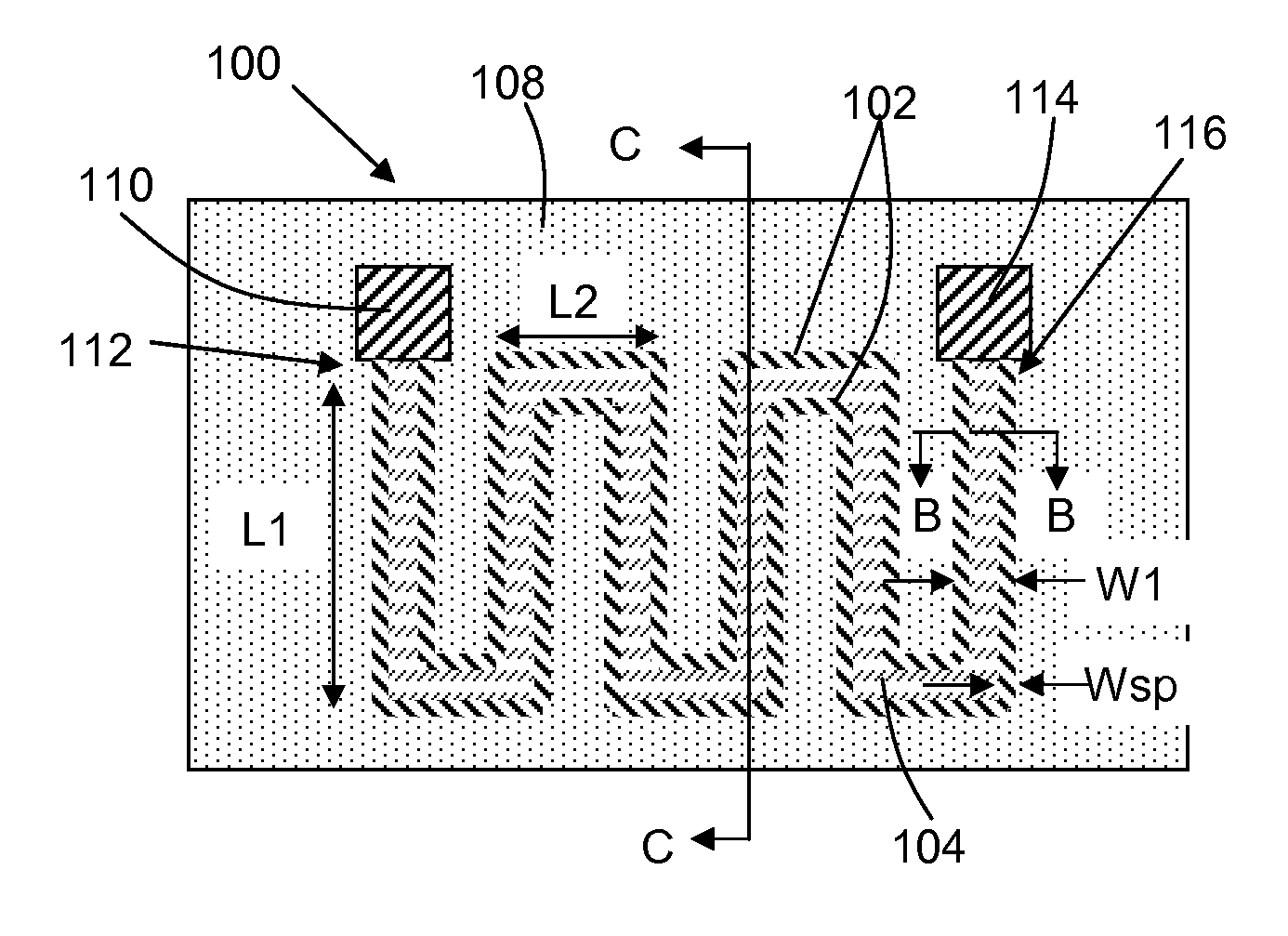
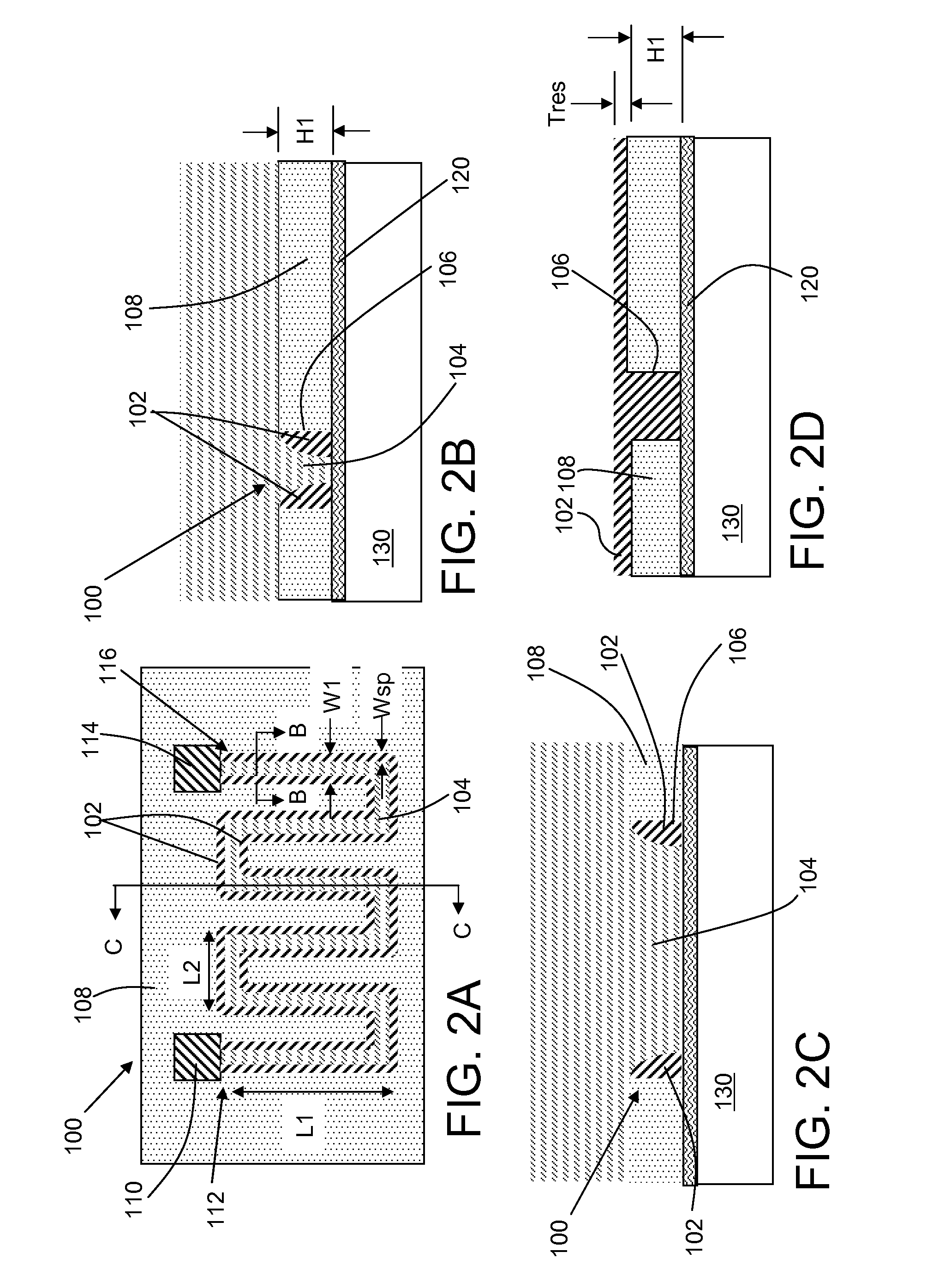
[0018]FIGS. 2A-2C show embodiments of a resistor 100 according to the disclosure. FIG. 2A shows a top view, FIG. 2B shows a cross-sectional view along line BB in FIG. 2A and FIG. 2C shows a cross-sectional view along line CC in FIG. 2A. Resistor 100 includes a pair of substantially parallel resistor material lengths 102 separated by a first dielectric 104. As shown in FIGS. 2B-2C, each resistor material length 102 is positioned adjacent to a sidewall of a trench 106 in a second dielectric 108. In addition, each resistor material length 102 may have a spacer shape, i.e., it is rounded as by etching rather than having a squared profile, and each resistor material length 102 may have a sub-lithographic dimension, e.g., width Wsp is less than current lithographic standards W1(approximately 50 nanometers). In one embodiment, resistor material lengths 102 each have a height H1 greater than width W1 thereof. Pair of substantially parallel resistor material lengths 102 may have a serpentine...


PUM


Abstract

A resistor and design structure including a pair of substantially parallel resistor material lengths separated by a first dielectric are disclosed. The resistor material lengths have a sub-lithographic dimension and may be spacer shaped.

Description

[0001]This application is related to U.S. Ser. No. ______, applicant docket number BUR920070238US1, filed ______.BACKGROUND[0002]1. Technical Field[0003]The disclosure relates generally to integrated circuit (IC) chips, and more particularly, to resistors for IC chips.[0004]2. Background Art[0005]In the integrated circuit (IC) chip fabrication industry, high resistivity value resistors are required. Typically, these resistors are formed by providing a thin layer of resistor material that is dimensioned to a particular length and width for a fixed thickness, which provides a known resistive value. FIG. 1A shows a top view and FIG. 1B shows a cross-sectional view of an illustrative resistor 10 having a length defined by a number of lengths L1 and a number of lengths L2 and a width W. Contacts 12 electrically couple resistor 10 to other circuitry (not shown). In order to provide the high resistive values, one approach enlarges (e.g., lengthens) the resistor. That is, the larger the num...

Claims


Application Information

Patent Timeline
Patent Type & Authority Applications(United States)
IPC IPC(8): H01C1/012G06F17/50
CPCH01C3/12G06F17/5045G06F30/30
Inventor HAKEY, MARK C.LUCE, STEPHEN E.NAKOS, JAMES S.
Owner GLOBALFOUNDRIES INC
Why Eureka
Try Eureka