Pattern measuring method and pattern measuring device

a pattern measuring and pattern technology, applied in the field of measuring methods, can solve the problems of determining the width and therefore not suiting detailed geometry evaluation, and achieving a smaller post-exposure pattern than expected, and achieve the effect of reducing the size of the post-exposure pattern

Active Publication Date: 2009-09-17
HITACHI HIGH-TECH CORP
View PDF3 Cites 18 Cited by
  • Summary
  • Abstract
  • Description
  • Claims
  • Application Information

AI Technical Summary

Benefits of technology

[0013]Forming a plurality of contours allows evaluation...

Problems solved by technology

An edge portion in an SEM image, however, has a certain width and hence does not suit detailed geometry evaluation.
In particular, when an edge is...

Method used


Image

  • Pattern measuring method and pattern measuring device
  • Pattern measuring method and pattern measuring device
  • Pattern measuring method and pattern measuring device

Examples


embodiments

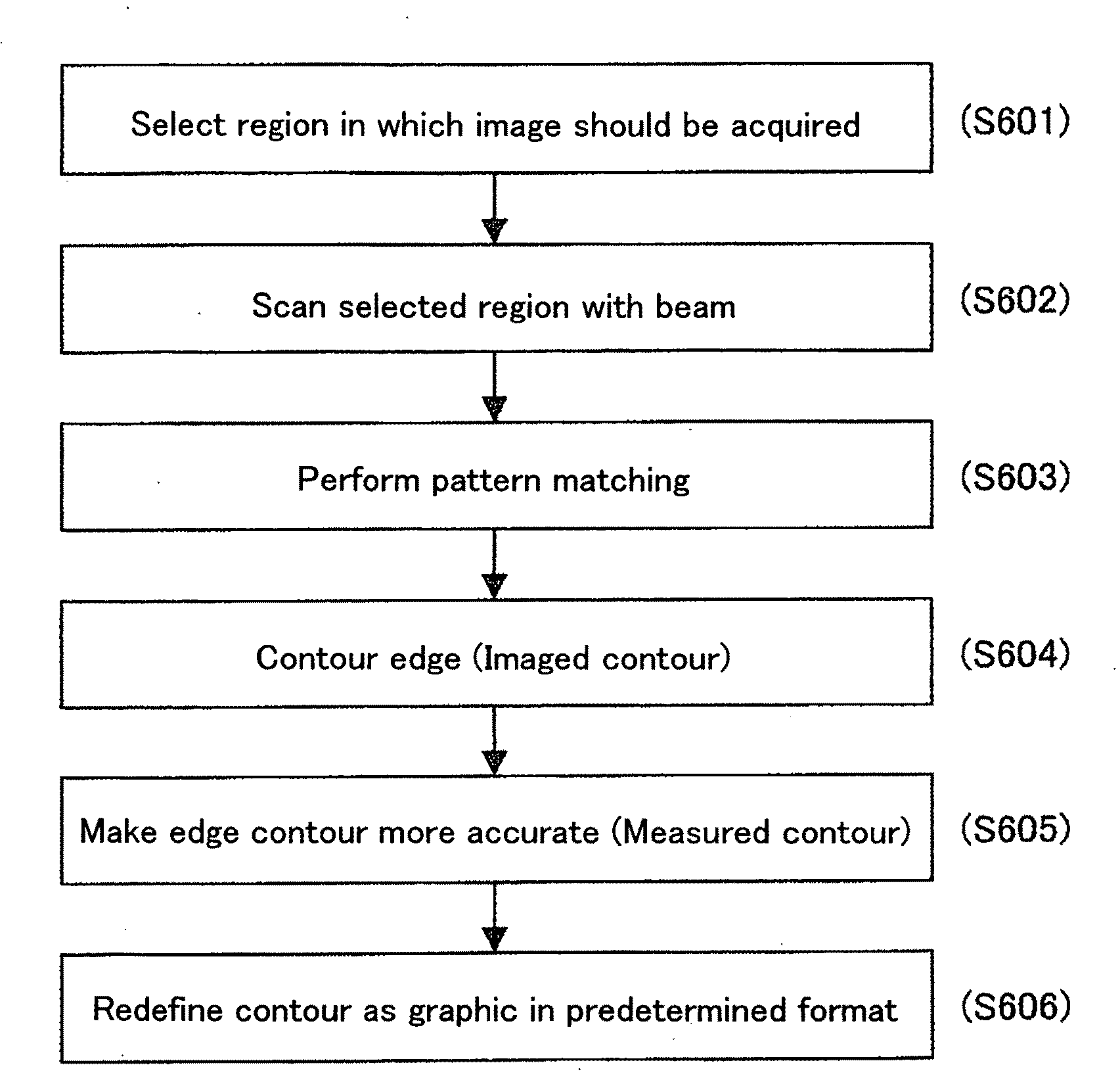
[0041]A description will be made of a method for evaluating taper (inclination) of an edge portion of a mask by using a plurality of contours obtained from an SEM image.

[0042]FIG. 3 explains an example of contouring an edge portion based on an SEM image of a certain portion of a mask. The solid line represents design data in a predetermined format (a GDS file, for example) and is expressed in the form of a diagram (hereinafter sometimes referred to as a design data diagram 301). The dash-dot line represents a contoured SEM edge obtained based on a predetermined method (hereinafter sometimes referred to as a first contour 302). The dash-dot-dot line represents another contoured SEM edge obtained based on the predetermined method (hereinafter sometimes referred to as a second contour 303).

[0043]The first contour 302 and the second contour 303 change their positions in accordance with the geometry of the edge portions at the upper and lower surface levels of the mask. For example, eval...


PUM


Abstract

An object of the present invention is to provide a sample measuring method and a sample measuring device suitable for evaluation of inclination of a pattern edge. To achieve the object, a method and a device for forming a plurality of contours of a pattern edge and evaluating the dimension between the contours are proposed below. Forming a plurality of contours allows evaluation of the degree of inclination of an edge portion of a pattern. Further, displaying evaluation values indicative of the degree of the inclination of the edge portion in an in-plane distribution form makes identifying the cause of taper formation easier.

Description

BACKGROUND OF THE INVENTION[0001]1. Field of the Invention[0002]The present invention relates to a method for measuring a pattern formed on a sample and a device for measuring the pattern, and particularly to a method and device for extracting a contour from a pattern edge in an image acquired with a scanning electron microscope or other device.[0003]2. Description of the Related Art[0004]In semiconductor manufacturing processes, a scanning electron microscope (hereinafter sometimes simply referred to as an SEM) or other charged particle beam device is used to measure a line width of a semiconductor device and evaluate the quality thereof. In particular, an SEM for measuring a line width of a line pattern and the diameter of a hole of a hole pattern of a semiconductor device is called a CD-SEM (Critical Dimension SEM).[0005]Conventionally, CD-SEM-based measurement has been used to obtain one-dimensional measurement results, which are pattern dimensions, but two-dimensional geometrie...

Claims


Application Information

Patent Timeline
IPC IPC(8): G06K9/48G06T7/00
CPCG06K9/4609G06T7/001G06T2207/30148G06T2207/10061G06T2207/20192G06T7/0083G06T7/12G06V10/443
Inventor MATSUOKA, RYOICHISUGIYAMA, AKIYUKI
Owner HITACHI HIGH-TECH CORP
Why Eureka
Try Eureka