Method of detecting a defect on an object

a defect detection and object technology, applied in the field of methods of detecting defects on objects, can solve the problems of significantly low reliability of the defect detection process, adversely affecting the resulting semiconductor device, etc., and achieve the effect of accurately detecting defects and detectability

Active Publication Date: 2009-09-24
SAMSUNG ELECTRONICS CO LTD
View PDF4 Cites 12 Cited by
  • Summary
  • Abstract
  • Description
  • Claims
  • Application Information

AI Technical Summary

Benefits of technology

[0018]According to the example embodiments, defects present in the inspection regions having different brightnesses may be detected using the properly obtained reference image. Thus, defect detectability with respect to the inspection regions is stabilized. As a result, defects present on the semiconductor substrate can be accurately detected.

Problems solved by technology

Each process can introduce various types of defects on the semiconductor substrate, which can adversely affect the resulting semiconductor device.
Thus, when defects present in inspection regions having different brightness properties are detected using only a single reference image, reliability of the defect detection process can be significantly low.

Method used


Image

  • Method of detecting a defect on an object
  • Method of detecting a defect on an object
  • Method of detecting a defect on an object

Examples


example embodiment 1

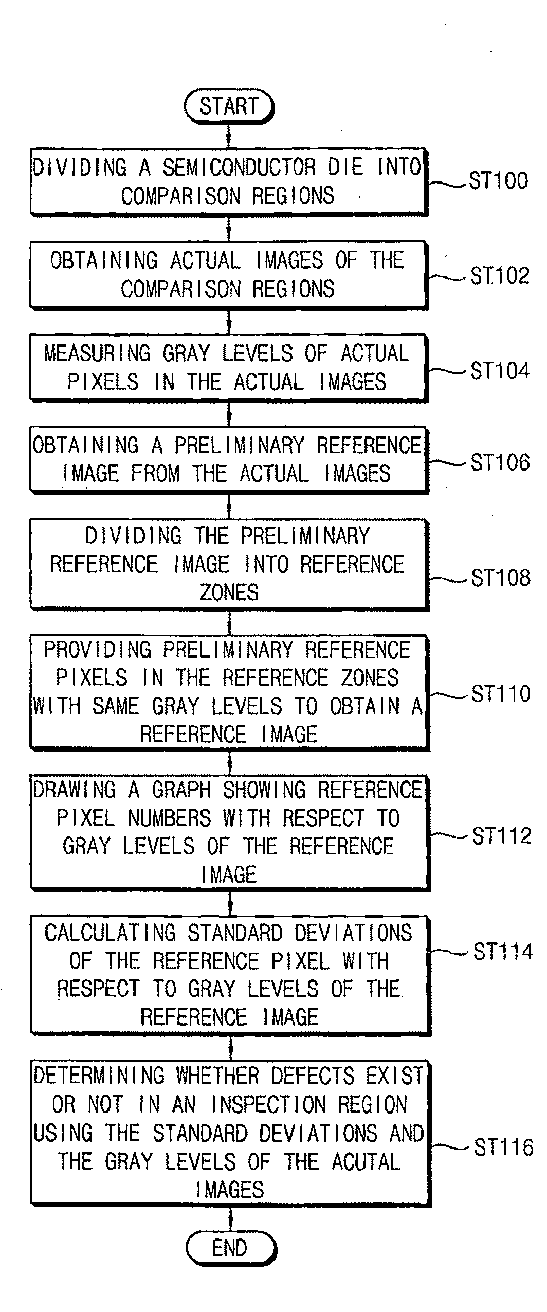
[0034]FIG. 1 is a flow chart illustrating a method of detecting a defect on an object in accordance with a first example embodiment of the present invention.

[0035]In this example embodiment, the object to which the method of detecting the defect may be applied can include a semiconductor die having a plurality of cells formed thereon. Further, the semiconductor die may include a cell region and a peripheral region configured to surround or encompass the cell region. Patterns can be repeatedly and regularly arranged in the cell region, while patterns can be irregularly arranged in the peripheral region.

[0036]Referring to FIG. 1, in step ST100, the semiconductor die can be divided into a plurality of comparison regions. In this example embodiment, the comparison regions can correspond to the cell region.

[0037]In step ST102, actual images of the comparison regions can be obtained. The actual images can be obtained by using light reflected from the comparison regions or by scanning the ...

example embodiment 2

[0050]FIG. 5 is a flow chart illustrating a method of detecting a defect on an object in accordance with a second example embodiment of the present invention.

[0051]In this example embodiment, the object to which the method of detecting the defect may be applied may include a semiconductor substrate where a plurality of dies may be formed. Further, the dies in a central portion, the dies in an edge portion and the dies in a middle portion of the semiconductor substrate may have different brightnesses.

[0052]Referring to FIG. 5, in step ST200, the semiconductor substrate may be divided into a plurality of comparison regions.

[0053]In step ST202, actual images of the comparison regions can be obtained.

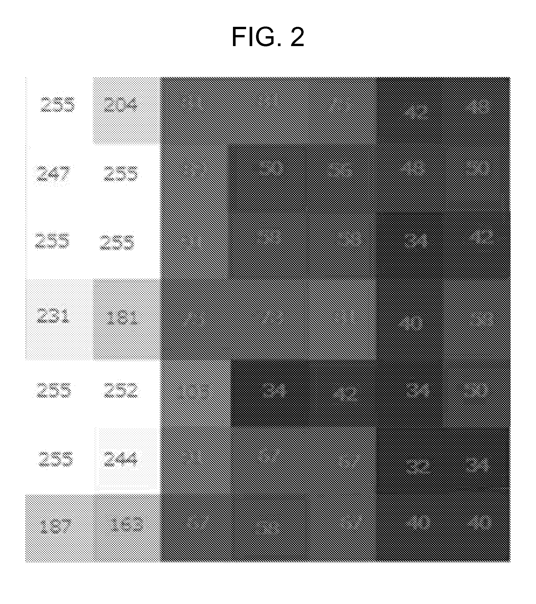
[0054]In step ST204, gray levels of the dies in the actual images can be measured.

[0055]In step ST206, a preliminary reference image is obtained from the actual images. In this example embodiment, gray level averages of each of the actual dies, which may be located proximal to substantially...


PUM


Abstract

In a method of detecting a defect on an object, a preliminary reference image can be obtained from a plurality of comparison regions defined on the object. The preliminary reference image is divided into reference zones by a similar brightness. Each of the reference zones is provided with substantially the same gray level, respectively, to obtain a reference image. Whether a defect exists in an inspection region in the comparison regions is determined using the reference image. Thus, defects in the inspection regions having different brightnesses can be detected using the properly obtained reference image.

Description

BACKGROUND[0001]1. Field[0002]Example embodiments relate to a method of detecting a defect on an object. More particularly, example embodiments relate to a method of detecting a defect generated, or otherwise present, on a semiconductor substrate.[0003]2. Description of the Related Art[0004]Generally, semiconductor devices are manufactured by various processes including a deposition process, a patterning process, a chemical mechanical polishing (CMP) process, a cleaning process, and other processes. Each process can introduce various types of defects on the semiconductor substrate, which can adversely affect the resulting semiconductor device. Therefore, a detection process for detecting the defects is performed so that decisions can be made for rectifying the defects, thereby improving device yield and reliability.[0005]According to a conventional method of defect detection, a semiconductor substrate can be divided into a plurality of inspection regions. An inspection image of an i...

Claims


Application Information

Patent Timeline
Patent Type & Authority Applications(United States)
IPC IPC(8): G06K9/00
CPCG06T2207/30148G06T7/0004H01L22/00
Inventor YANG, YU-SINSONG, KYUNG-SUKKIM, JI-HAEJUN, CHUNG-SAM
Owner SAMSUNG ELECTRONICS CO LTD
Why Eureka
Try Eureka