Semiconductor device and method for fabricating the same

a semiconductor and device technology, applied in the direction of semiconductor devices, basic electric elements, electrical equipment, etc., can solve the problem ofconsiderably technical difficulties in fabricating semiconductor devices, and achieve the effect of improving the drive capability of semiconductor devices

Active Publication Date: 2009-10-01
PANNOVA SEMIC
View PDF20 Cites 62 Cited by
  • Summary
  • Abstract
  • Description
  • Claims
  • Application Information

AI Technical Summary

Benefits of technology

[0018]According to the semiconductor device of the present invention and its method of fabrication, a silicon mixed crystal layer for generating stress in a channel region of an active region can be formed in a satisfactorily controlled manner, thereby making it possible to improve the drive capability of the semiconductor device.

Problems solved by technology

It is considerably technically difficult to fabricate semiconductor devices having a minimum feature size of 65 nm or less.

Method used


Image

  • Semiconductor device and method for fabricating the same
  • Semiconductor device and method for fabricating the same
  • Semiconductor device and method for fabricating the same

Examples


first embodiment

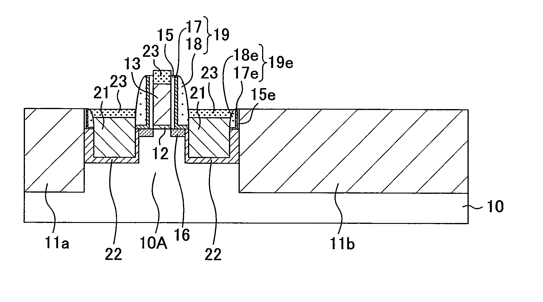
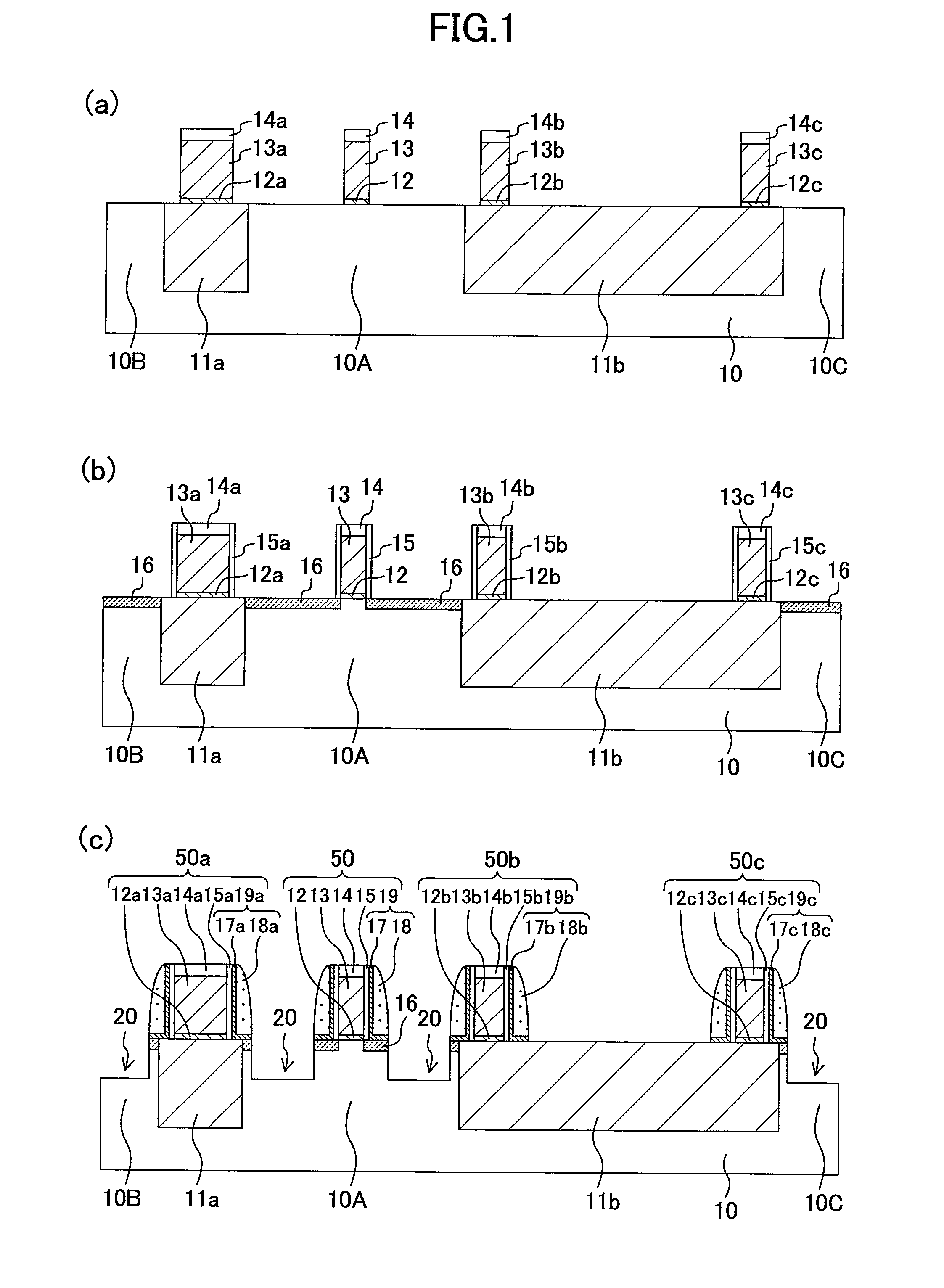
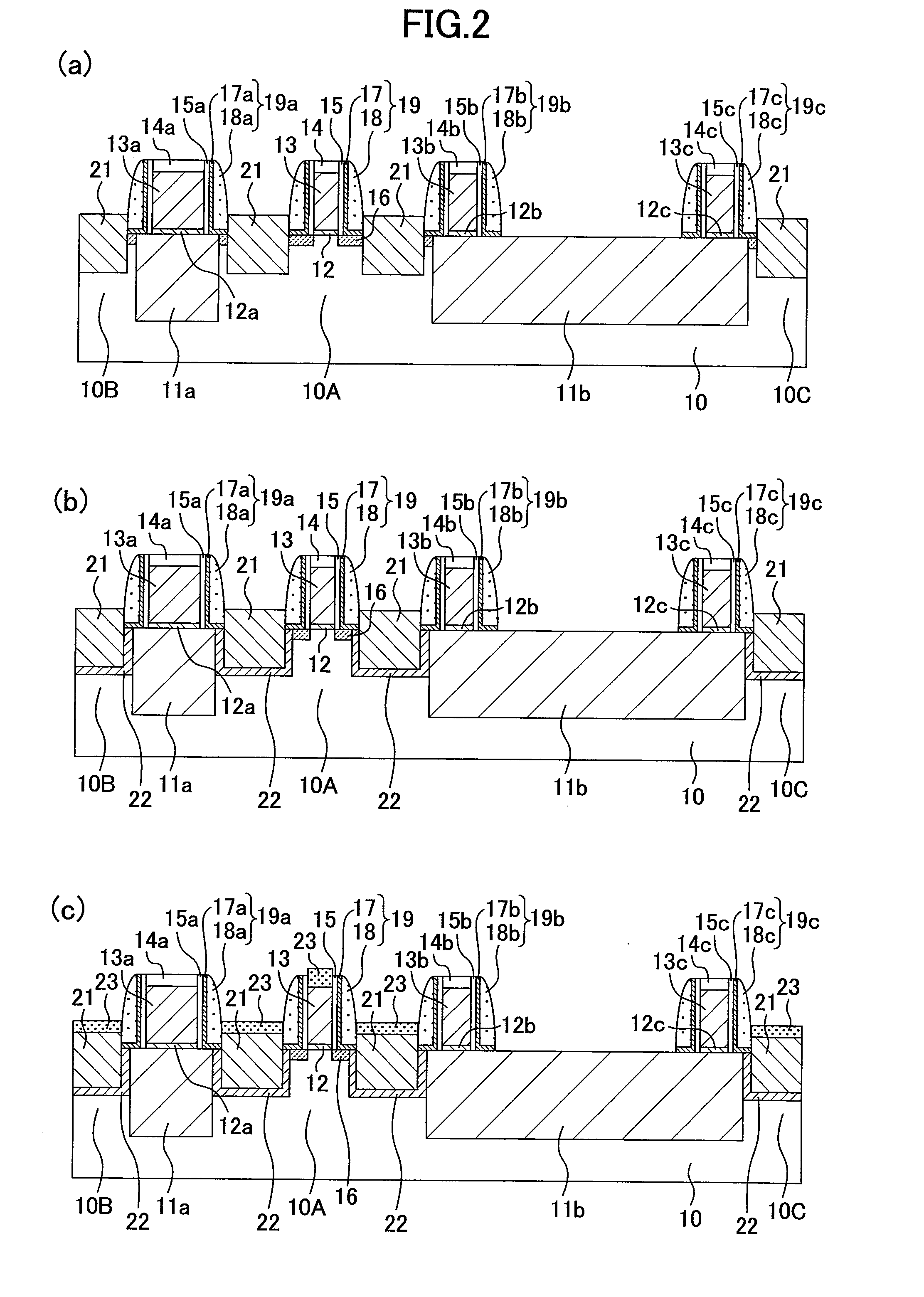
[0057]A method for fabricating a semiconductor device according to a first embodiment of the present invention will be described with reference to the drawings. FIGS. 1(a) to 1(c) and FIGS. 2(a) to (c) are cross-sectional views showing the method for fabricating the semiconductor device of this embodiment.

[0058]Initially, as shown in FIG. 1(a), trenches are formed in an upper portion of a semiconductor substrate 10 made of silicon (Si) with a main surface having, for example, a (100) plane orientation by, for example, STI (Shallow Trench Isolation). The trenches are filled with an insulating film to selectively form isolation regions 11a and 11b. As a result, active regions 10A, 10B and 10C that are made of the semiconductor substrate 10 and are surrounded by the isolation regions 11a and 11b are formed. Here, an isolation width of the isolation region 11a is narrower than that of the isolation region 11b, and is twice to five times as long as a gate length of a gate electrode as a ...

second embodiment

[0105]A method for fabricating a semiconductor device according to a second embodiment of the present invention will be described with reference to the drawings. FIGS. 6 and 7 are cross-sectional views showing the method for fabricating the semiconductor device of this embodiment. Note that the same parts as those of the first embodiment (FIGS. 1 and 2) are indicated by the same reference characters and will not be described in more detail.

[0106]Initially, as shown in FIG. 6(a), trenches are formed in an upper portion of a semiconductor substrate 10 made of silicon (Si) with a main surface having, for example, a (100) plane orientation by, for example, STI (Shallow Trench Isolation). The trenches are filled with an insulating film to selectively form isolation regions 11a and 11b. As a result, an active region 10A that is made of the semiconductor substrate 10 and is surrounded by the isolation regions 11a and 11b are formed.

[0107]Next, an n-type well region (not shown) is formed by...

third embodiment

[0125]A method for fabricating a semiconductor device according to a third embodiment of the present invention will be described with reference to the drawings. FIGS. 9 and 10 are cross-sectional views showing the method for fabricating the semiconductor device of this embodiment. Note that the same parts as those of the first embodiment (FIGS. 1 and 2) are indicated by the same reference characters and will not be described in more detail.

[0126]Initially, as shown in FIG. 9(a), a gate insulating film 12, a gate electrode 13 and a protective insulating film 14 are formed on an active region 10A surrounded by isolation regions 11a and 11b in a semiconductor substrate 10 in a manner similar to the step of FIG. 6(a) in the second embodiment. Next, offset spacers 15 are formed on side surfaces of the gate electrode 13, and thereafter, p-type extension regions 16 are formed in regions on sides of the gate electrode 13 of the active region 10A.

[0127]Next, as shown in FIG. 9(b), for exampl...


PUM


Abstract

A semiconductor device includes an isolation region (11a) formed in a semiconductor substrate (10), an active region made of the semiconductor substrate (10) surrounded by the isolation region (11a) and having a trench portion, a MIS transistor of a first-conductivity type having a gate electrode (13) formed on the active region, a first sidewall (19) formed on a side surface of the gate electrode between the gate electrode (13) and the trench portion as viewed in the top, and a silicon mixed crystal layer (21) of the first-conductivity type, the trench portion being filled with the silicon mixed crystal layer (21) of the first-conductivity type, a substrate region provided between the trench portion and the isolation region (11a, 11b) and made of the semiconductor substrate (10), and an impurity region (22) of the first-conductivity type formed in the substrate region. The silicon mixed crystal layer (21) generates stress in a channel region of the active region.

Description

TECHNICAL FIELD[0001]The present invention relates to a semiconductor device having a MIS (Metal Insulator Semiconductor) transistor and its method of fabrication.BACKGROUND ART[0002]In order to improve properties of a semiconductor device, such as operation, power consumption, packing density and the like, a minimum feature size has been reduced. It is considerably technically difficult to fabricate semiconductor devices having a minimum feature size of 65 nm or less. The improvement of the properties only by miniaturization is approaching its limit.[0003]To avoid this, a so-called strained silicon transistor has attracted attention as a transistor whose properties are improved even without miniaturization. The strained silicon transistor is a MIS transistor in which the mobility of carriers is increased by applying stress (strain) to the channel region (see, for example, Patent Documents 1 and 2).[0004]For example, in the case of a p-type MIS transistor, when compressive stress is...

Claims


Application Information

Patent Timeline
Patent Type & Authority Applications(United States)
IPC IPC(8): H01L29/78H01L21/336
CPCH01L21/823412H01L21/823418H01L21/823481H01L21/823807H01L21/823814H01L29/7848H01L29/165H01L29/665H01L29/66628H01L29/66636H01L29/7833H01L21/823878
Inventor SUZUKI, KENSUZUKI, JUN
Owner PANNOVA SEMIC
Why Eureka
Try Eureka