
Eureka
For R&D, Eureka makes reading and utilizing patents & technical documents easy.
Eureka AIR
Designed for self-driven R&D workflows. Generate viable solutions, solve complex R&D challenges, empower your innovation with AI.

Eureka Materials
Designed for material experts only. Revolutionize your material R&D, from search, analyze, to developing new materials.

TechResearch
Generate reliable direction feasibility study reports for your R&D in just a few steps.

TechSeek
Discover and master advanced knowledge NOW. Basics, ideas, possibilities, all at once.

TechMind
As an expert in R&D Theories, TechMind can generates customized viable solutions instantly.

TechRisk
Analyze your overall solution with one click, know your potential R&D risks in advance.

TechMonitor
Get weekly tech updates, stay abreast of the latest tech innovations and key insights.
Varistor
- Summary
- Abstract
- Description
- Claims
- Application Information
AI Technical Summary
Benefits of technology
Problems solved by technology
Method used
Image

Examples
first modification example
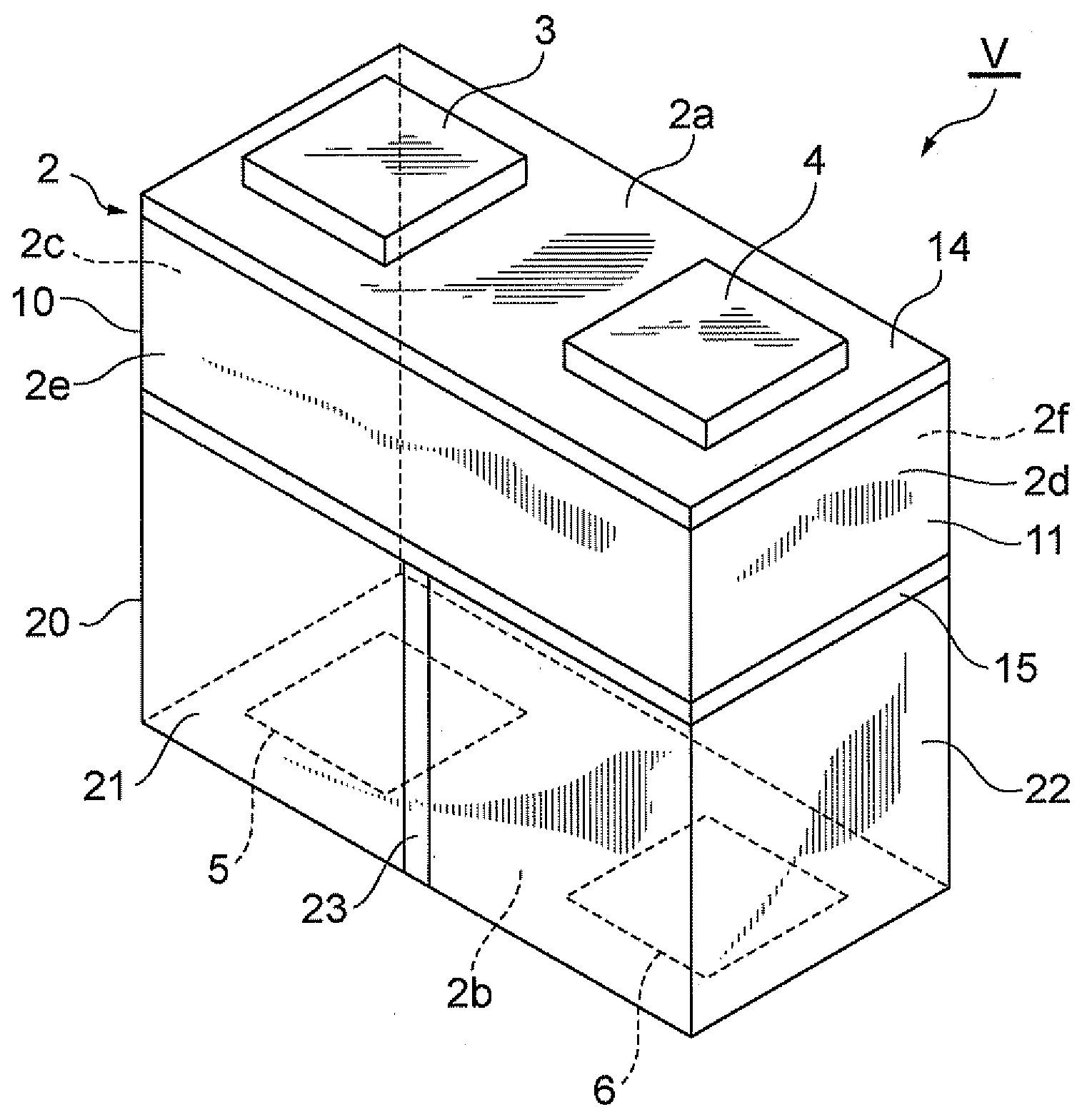
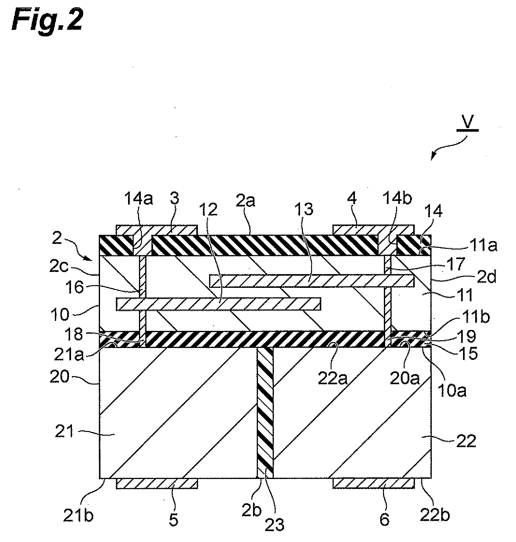
[0052]In the foregoing embodiment the side faces of the first and second heat radiation portions 21, 22 are exposed, but they may be covered by an insulator, as shown in FIG. 3. FIG. 3(a) is a schematic sectional view of the varistor according to the first modification example and FIG. 3(b) a plan view from the side of the second face 2b of the element body 2. The varistor Va of the first modification example is so configured that the heat radiation section 20 further has an insulating layer 24 to cover the side faces of the first and second heat radiation portions 21, 22.
[0053]The insulating layer 24 constitutes some areas of the side faces 2c-2f of the element body 2 in the heat radiation section 20. In this case, electrical insulation from surrounding parts is certainly achieved in a mounted state of the varistor of the present invention.
[0054]For producing the varistor Va of the first modification example, the heat radiation green sheets are formed by applying the slurry for the...
second modification example
[0056]The foregoing embodiment is the example wherein the first and second external electrodes 3, 4 are connected to the electronic device and wherein the third and fourth external electrodes 5, 6 are connected to the substrate, but it can also be contemplated that the third and fourth external electrodes 5, 6 are connected to the electronic device and the first and second external electrodes 3, 4 are connected to the substrate.
[0057]As shown in FIG. 4, the varistor Vb of the second modification example is preferably provided with an insulating layer 25 to cover the face of the first and second heat radiation portions facing the electronic device. The insulating layer 25 constitutes the second face 2b of the element body 2. Apertures 25a, 25b penetrating the insulating layer 25 in the thickness direction are formed in the insulating layer 25 and the third and fourth external electrodes 5, 6 are arranged so as to cover the apertures 25a, 25b, respectively. This makes the third extern...
third modification example
[0059]In the foregoing embodiment the first varistor electrode 12 and the second varistor electrode 13 are arranged so as to face each other in the varistor element body 11, but the configuration of the varistor electrodes does not always have to be limited to it. As shown in FIG. 5, the varistor Vc of the third modification example is provided with first to third varistor electrodes 31-33, instead of the first and second varistor electrodes of the varistor V of the above embodiment. The first and second varistor electrodes 31, 32 are arranged in a mutually insulated state on the face 11a of the varistor element body 11. The third varistor electrode 33 is arranged inside the varistor element body 11 so as to face the first and second varistor electrodes 31, 32.
[0060]The first varistor electrode 31 is physically and electrically connected to one end of the through-hole electrode 16 exposed in the face 11a of the varistor element body 11 and the second varistor electrode 32 is physica...
PUM
 Abstract
Description
Claims
Application Information
 - R&D Engineer
- R&D Manager
- IP Professional
- Industry Leading Data Capabilities
- Powerful AI technology
- Patent DNA Extraction
Browse by: Latest US Patents, China's latest patents, Technical Efficacy Thesaurus, Application Domain, Technology Topic, Popular Technical Reports.
© 2024 PatSnap. All rights reserved.Legal|Privacy policy|Modern Slavery Act Transparency Statement|Sitemap|About US| Contact US: help@patsnap.com