

Optical package
a technology of optical packages and optical waveguides, applied in the direction of electrical apparatus construction details, semiconductor lasers, instruments, etc., can solve the problems of difficult optical alignment between an external laser or connector and an on-die optical waveguide, slow and intricate active alignment, and special skills
- Summary
- Abstract
- Description
- Claims
- Application Information
AI Technical Summary
Problems solved by technology
Method used
Image

Examples
Embodiment Construction
[0013]In the following detailed description, numerous specific details are set forth in order to provide a thorough understanding of the invention. However it will be understood by those of ordinary skill in the art that the present invention may be practiced without these specific details. In other instances, well-known methods, procedures, components and circuits have not been described in detail so as not to obscure the present invention.
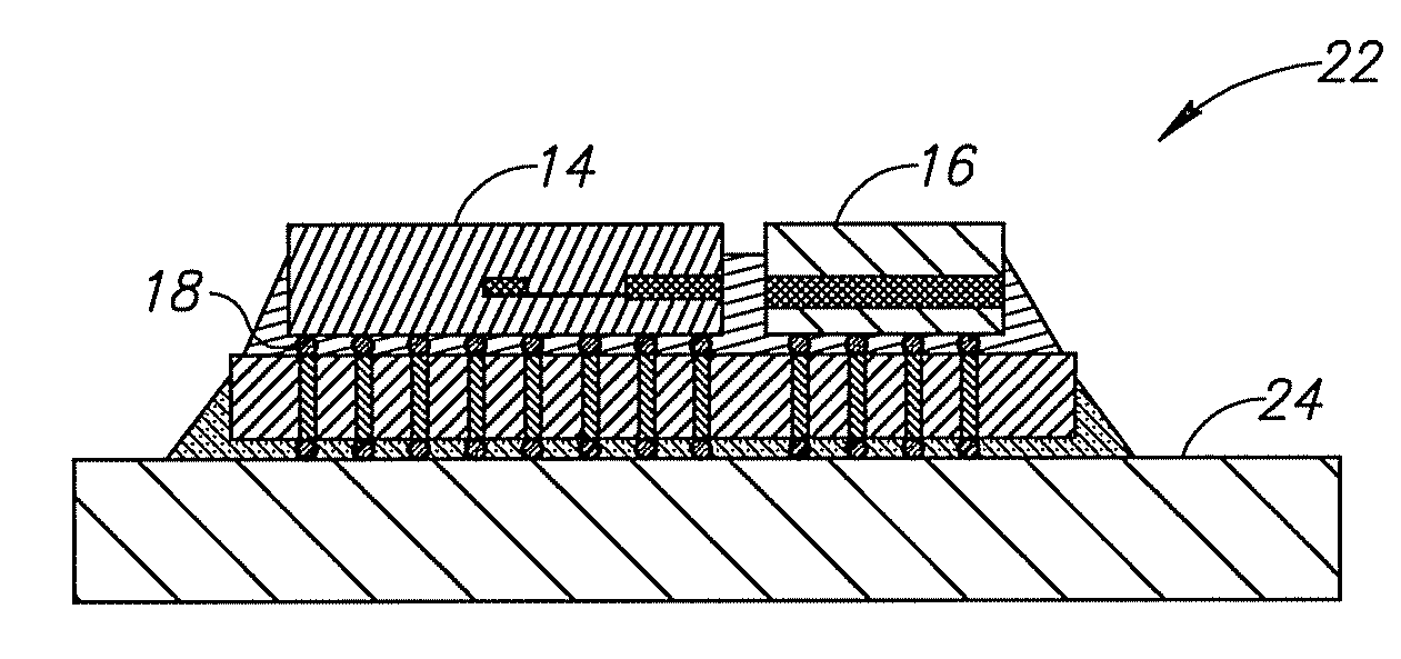
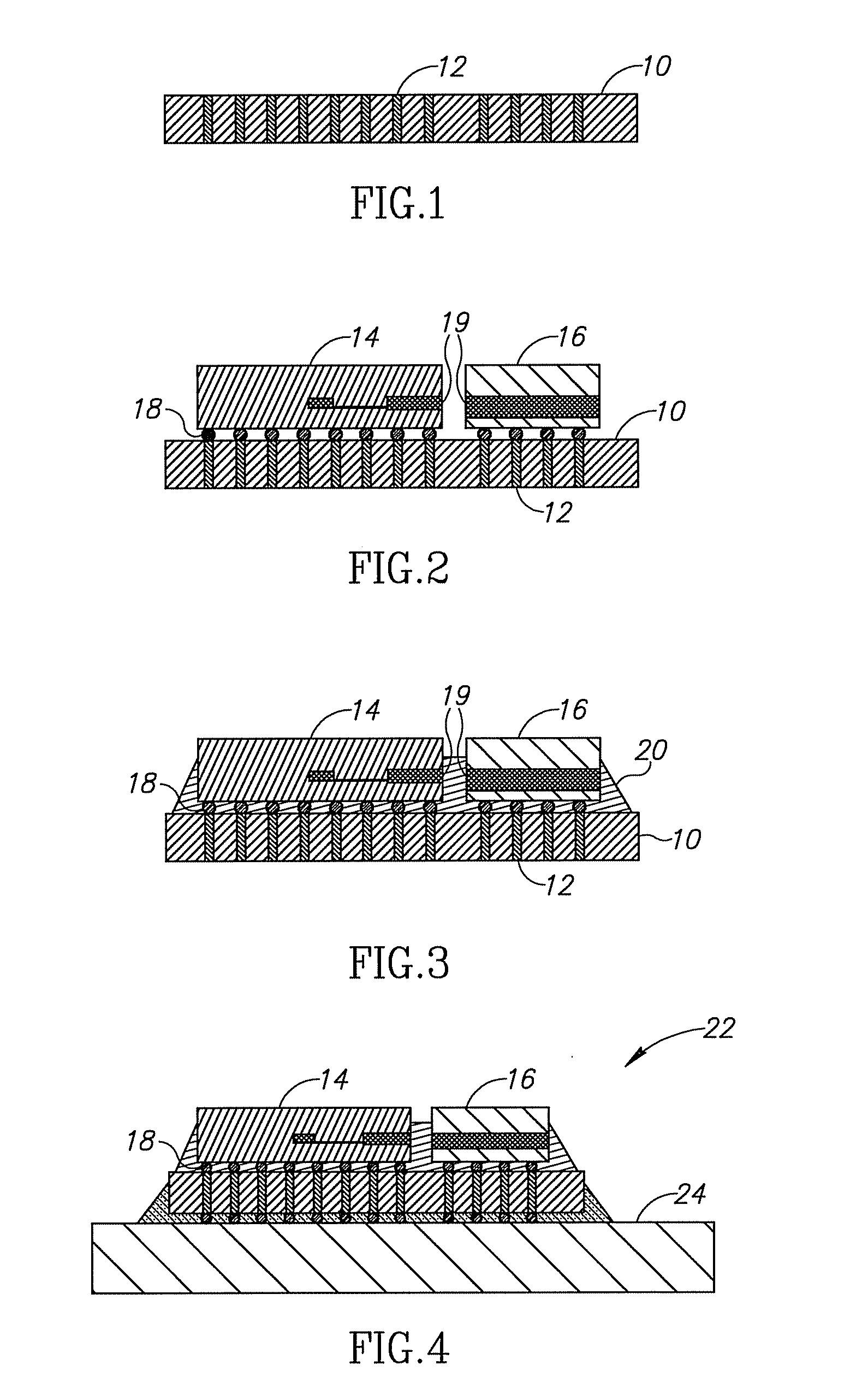
[0014]Solder self-alignment can provide a positional alignment precision of less than 2 μm as it is known. It is suggested, according to some embodiments of the present invention, to fabricate traces and pads on a silicon interposer using, for example, lithography, which may provide very tight tolerance control. The volume of the solder bumps may be precisely controlled, for example, by evaporation or plating the solder so that the standoff height of the solder joints of the dies over the interposer can be precisely controlled and good z-axis opt...
PUM
| Property | Measurement | Unit |
|---|---|---|
| Electric potential / voltage | aaaaa | aaaaa |
| Electric properties | aaaaa | aaaaa |
Abstract
Description
Claims
Application Information