Multi-Layer Method for Formation of Registered Arrays of Cylindrical Pores in Polymer Films

a polymer film and array technology, applied in the direction of resistive material coating, cable/conductor manufacturing, metallic material coating process, etc., can solve the problems of reducing the aspect ratio of mask openings and subsequently etched lines or other openings in the substrate, affecting the effect of lithographic processing methods, and affecting the quality of lithographic processing

Active Publication Date: 2009-10-22
MICRON TECH INC
View PDF99 Cites 75 Cited by
  • Summary
  • Abstract
  • Description
  • Claims
  • Application Information

AI Technical Summary

Problems solved by technology

Making electrical contacts to conductive lines has become a significant challenge as the dimensions of semiconductor features shrink to sizes that are not easily accessible by conventional lithography.
Optical lithographic processing methods have difficulty fabricating structures and features at the sub-30 nanometer level.
However, in some applications, the polymer block that is removed does not extend completely through the film and requires an additional etch of material to expose the underlying substrate, resulting in a reduction in the aspect ratio of the mask openings and the subsequently etched line or other opening in the substrate.

Method used


Image

  • Multi-Layer Method for Formation of Registered Arrays of Cylindrical Pores in Polymer Films
  • Multi-Layer Method for Formation of Registered Arrays of Cylindrical Pores in Polymer Films
  • Multi-Layer Method for Formation of Registered Arrays of Cylindrical Pores in Polymer Films

Examples


Embodiment Construction

[0014]The following description with reference to the drawings provides illustrative examples of devices and methods according to embodiments of the invention. Such description is for illustrative purposes only and not for purposes of limiting the same.

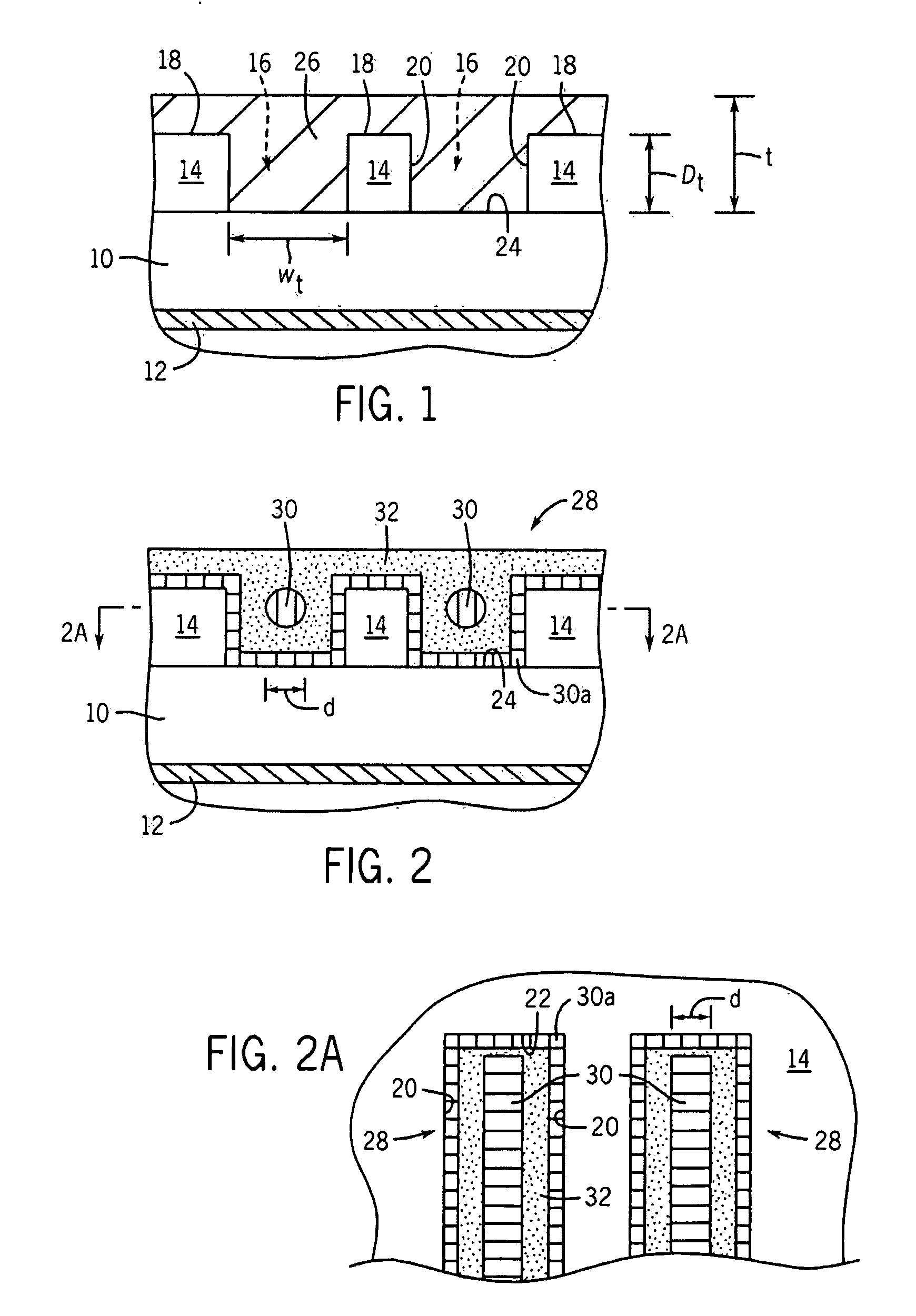
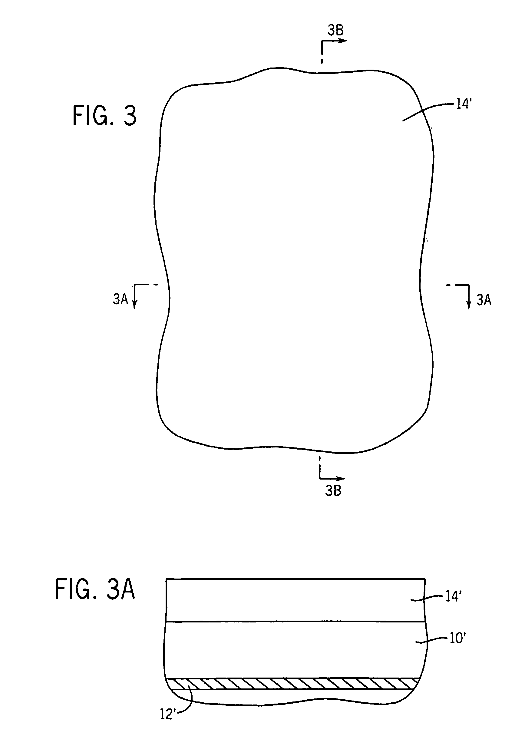
[0015]In the context of the current application, the term “semiconductor substrate” or “semiconductive substrate” or “semiconductive wafer fragment” or “wafer fragment” or “wafer” will be understood to mean any construction comprising semiconductor material, including but not limited to bulk semiconductive materials such as a semiconductor wafer (either alone or in assemblies comprising other materials thereon), and semiconductive material layers (either alone or in assemblies comprising other materials). The term “substrate” refers to any supporting structure including, but not limited to, the semiconductive substrates, wafer fragments or wafers described above.

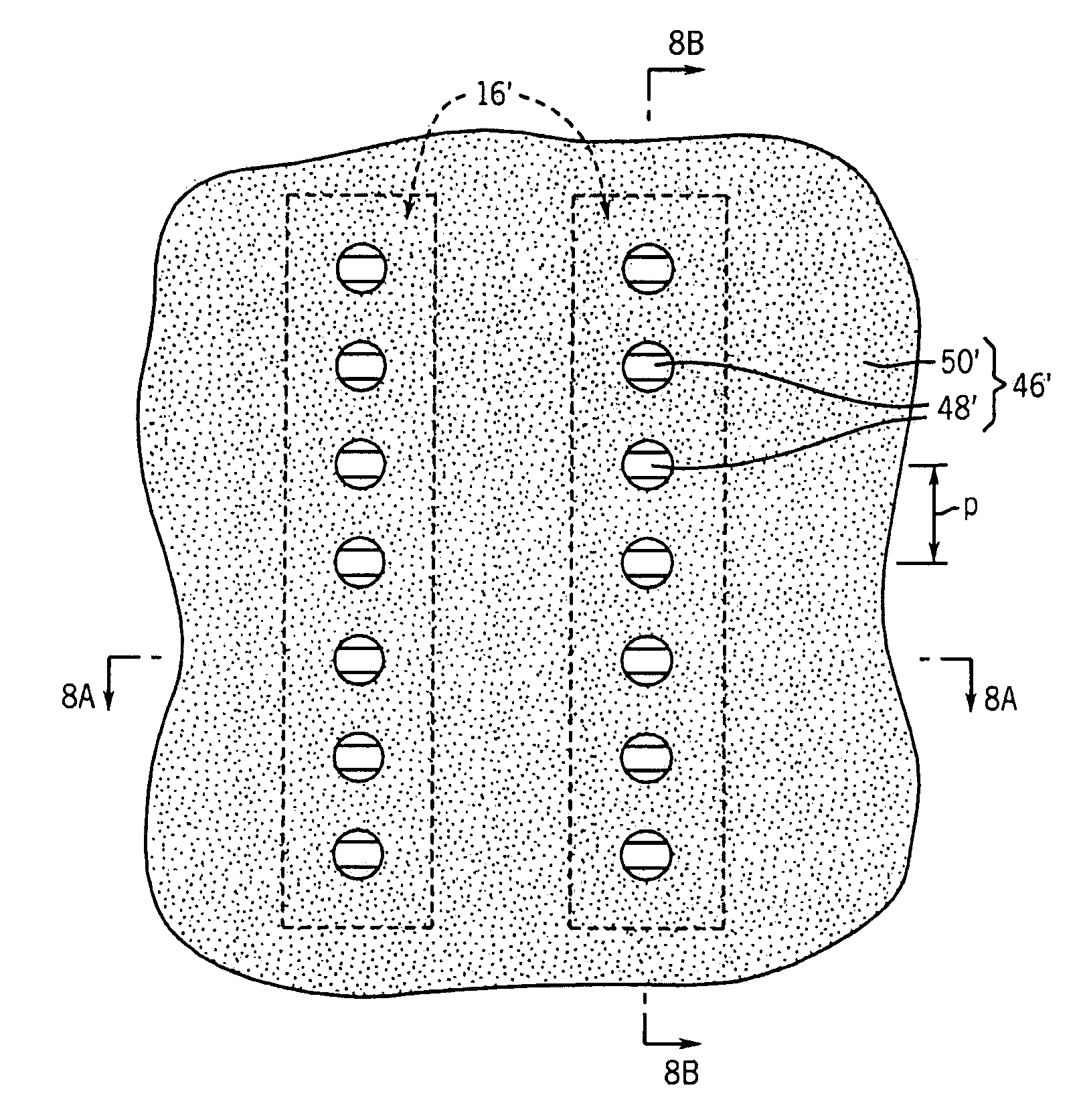
[0016]“Lo” as used herein is the inherent periodicity or pitch value (bul...


PUM

PropertyMeasurementUnit
feature sizeaaaaaaaaaa
diameteraaaaaaaaaa
widthaaaaaaaaaa

Abstract

Methods for fabricating sublithographic, nanoscale polymeric microstructures utilizing self-assembling block copolymers, and films and devices formed from these methods are provided.

Description

TECHNICAL FIELD[0001]Embodiments of the invention relate to methods of fabricating thin films of self-assembling block copolymers, and devices resulting from those methods.BACKGROUND OF THE INVENTION[0002]As the development of nanoscale mechanical, electrical, chemical and biological devices and systems increases, new processes and materials are needed to fabricate nanoscale devices and components. Making electrical contacts to conductive lines has become a significant challenge as the dimensions of semiconductor features shrink to sizes that are not easily accessible by conventional lithography. Optical lithographic processing methods have difficulty fabricating structures and features at the sub-30 nanometer level. The use of self assembling diblock copolymers presents another route to patterning at nanoscale dimensions. Diblock copolymer films spontaneously assemble into periodic structures by microphase separation of the constituent polymer blocks after annealing, for example by...

Claims


Application Information

Patent Timeline
Patent Type & Authority Applications(United States)
IPC IPC(8): B05D5/12B44C1/22B32B3/00
CPCB05D1/34B05D3/0254B05D5/02Y10S977/888Y10S977/90Y10T428/24612Y10S438/947Y10T428/24174Y10T428/2462Y10T428/24182Y10S977/895G03F7/0002
Inventor MILLWARD, DAN B.
Owner MICRON TECH INC
Why Eureka
Try Eureka