Semiconductor chip and manufacturing method for the same, and semiconductor device

a semiconductor and chip technology, applied in the direction of semiconductor devices, semiconductor/solid-state device details, electrical apparatus, etc., can solve the problems of electrical short circuit and lower connection reliability

Active Publication Date: 2005-07-14
KIOXIA CORP +3
View PDF5 Cites 235 Cited by
  • Summary
  • Abstract
  • Description
  • Claims
  • Application Information

AI Technical Summary

Problems solved by technology

Furthermore, if an activator such as a flux is used for removing the oxide film, migration due to impure ions caused by the activator occurs and this may cause an electrical shortcir...

Method used


Image

  • Semiconductor chip and manufacturing method for the same, and semiconductor device
  • Semiconductor chip and manufacturing method for the same, and semiconductor device
  • Semiconductor chip and manufacturing method for the same, and semiconductor device

Examples


first embodiment

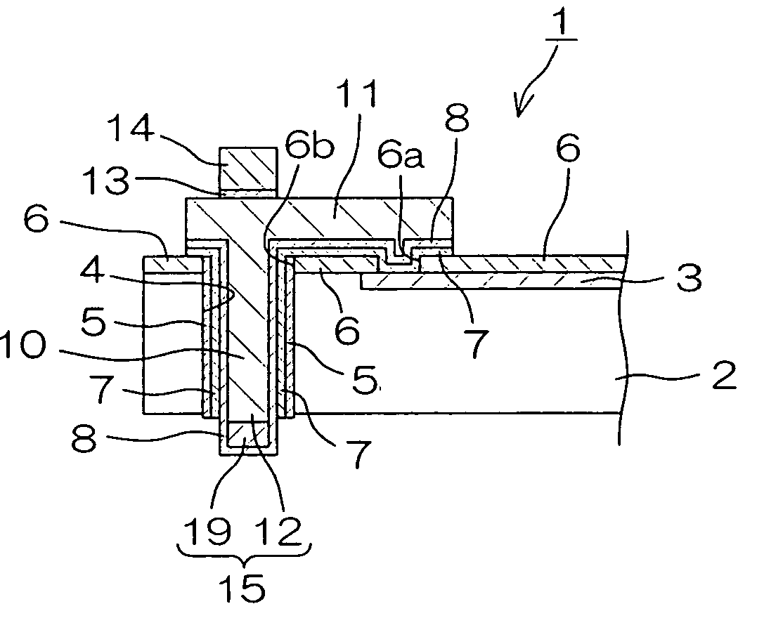
[0119]FIG. 1 is an illustrative sectional view showing the structure of a semiconductor chip relating to the invention.

[0120] This semiconductor chip 1 includes a semiconductor substrate 2 made of silicon (Si). On one surface (hereinafter, referred to as “front surface”) of the semiconductor substrate 2, a function device 3 having a plurality of electrodes is formed. By the side of the function device 3, a through hole 4 penetrating the semiconductor substrate 2 in the thickness direction is formed.

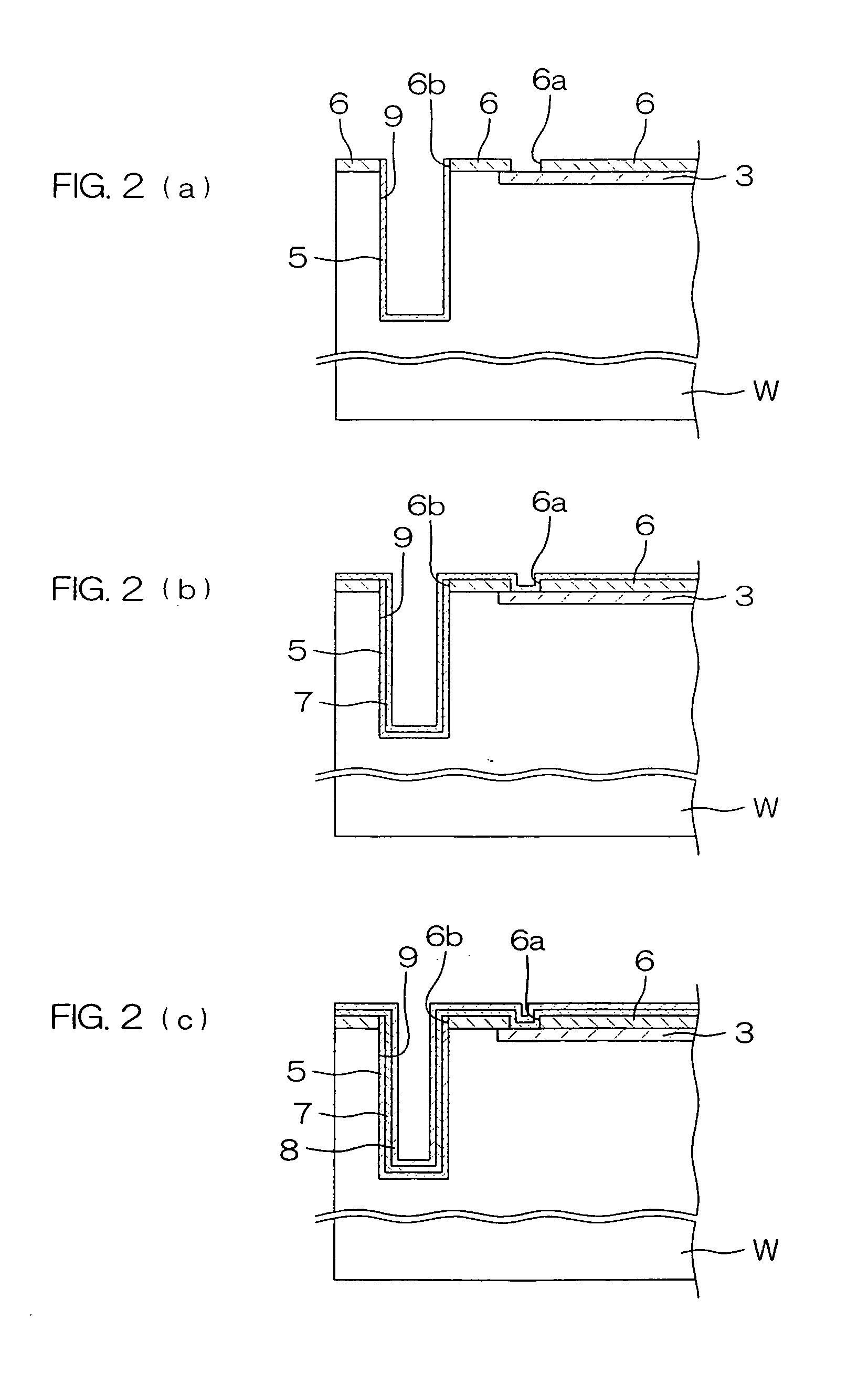
[0121] On the front surface of the semiconductor substrate 2, a hard mask 6 having openings 6a and 6b is formed. The hard mask 6 is made of silicon oxide (SiO2). In a vertical top plan view of the semiconductor substrate 2, the electrode of the function device 3 exists inside the opening 6a. The opening 6b and the through hole 4 forms one hole having a continuous inner wall surface.

[0122] On the inner wall surface of the through hole 4 and the opening 6b, an insulating film 5 made of si...

second embodiment

[0158]FIG. 3 is an illustrative sectional view of a semiconductor chip relating to the invention. In FIG. 3, portions corresponding to the parts of the semiconductor chip 1 shown in FIG. 1 are attached with the same reference symbols as in FIG. 1 and description thereof is omitted.

[0159] This semiconductor chip 21 has a structure similar to that of the semiconductor chip 1, however, the rear side protruding electrode 22 does not include the low melting point metal layer 19 (see FIG. 1), and the entirety of the rear side protruding electrode 22 is made of the same kind of material as that of the penetrating electrode 10 (copper, tungsten, aluminum, or an alloy of these). The penetrating electrode 10 and the rear side protruding electrode 22 are formed integrally. The rear side protruding electrode 22 is covered by the oxidation preventive film 8 like the rear side protruding electrode 15 of the semiconductor chip 1.

[0160] By joining the rear side protruding electrode 22 to an electr...

third embodiment

[0165]FIG. 5 is an illustrative sectional view showing the structure of a semiconductor chip relating to the invention. In FIG. 5, portions corresponding to the parts of the semiconductor chip 21 shown in FIG. 3 are attached with the same reference symbols as in FIG. 3 and description thereof is omitted.

[0166] This semiconductor chip 25 has a structure similar to that of the semiconductor chip 21 shown in FIG. 3, however, between the oxidation preventive film 8 and the penetrating electrode 10 and between the oxidation preventive film 8 and the interconnection member 11, an intermetallic diffusion preventive film 26 is interposed. The intermetallic diffusion preventive film 26 is made of titanium tungsten or titanium.

[0167] When the metal forming the oxidation preventive film 8 and the metal forming the penetrating electrode 10 and the interconnection member 11 easily react with each other, for example, when the oxidation preventive film 8 is made of gold, and the penetrating elect...


PUM


Abstract

The invention provides a semiconductor chip manufacturing method including the steps of: forming a concave portion extended in the thickness direction of a semiconductor substrate which has a front surface and a rear surface and has a function device formed on the front surface, from the front surface; forming an oxidation preventive film made of an inert first metal material by supplying the first metal material onto the inner wall surface of the concave portion; supplying a second metal material containing a metal which is oxidized more easily than the first metal material to the inside of the concave portion after the step of forming the oxidation preventive film; electrically connecting the second metal material supplied to the inside of the concave portion and the function device; and thinning the semiconductor substrate so that the thickness thereof becomes thinner than the depth of the concave portion by removing the semiconductor substrate from the rear surface while leaving the oxidation preventive film.

Description

BACKGROUND OF THE INVENTION [0001] 1. Field of the Invention [0002] This invention relates to semiconductor chip having protruding electrode and manufacturing method for the same, and multi-chip semiconductor device equipped with a plurality of semiconductor chips having protruding electrodes. [0003] 2. Description of Related Art [0004]FIG. 20 is an illustrative sectional view showing the structure of a semiconductor chip having a conventional penetrating electrode. [0005] This semiconductor chip 91 includes a semiconductor substrate 90 made of silicon (Si). On one surface (hereinafter, referred to as “front surface”) of the semiconductor substrate 90, a function device 71 having a plurality of electrodes is formed. By the side of the function device 71, a through hole 79 penetrating the semiconductor substrate 90 in the thickness direction is formed. [0006] On the front surface of the semiconductor substrate 90, a hard mask 72 having openings 72a and 72b is formed. The hard mask 72...

Claims


Application Information

Patent Timeline
IPC IPC(8): H01L21/28H01L21/3205H01L23/52H01L21/44H01L21/46H01L21/60H01L21/768H01L23/12H01L23/48H01L23/544H01L25/00H01L25/065
CPCH01L21/76843H01L2924/0002H01L23/481H01L25/0657H01L25/50H01L2224/16145H01L2224/48247H01L2225/0651H01L2225/06513H01L2225/06517H01L2225/06541H01L2225/06582H01L2225/06586H01L2924/01029H01L2924/01046H01L2924/01078H01L2924/01079H01L2924/04941H01L2924/12044H01L2924/15311H01L24/48H01L2924/01322H01L2924/01327H01L24/05H01L2224/48463H01L2224/73257H01L2924/00014H01L21/76898H01L2224/05554H01L2224/16146H01L2224/13025H01L24/03H01L24/11H01L24/13H01L24/16H01L2224/02372H01L2224/0401H01L2224/04042H01L2224/05548H01L2224/0557H01L2224/45099H01L2224/05552H01L2224/05569H01L2924/181H01L2924/12042H01L2924/00H01L2924/00012H01L21/60
Inventor TANIDA, KAZUMASAUMEMOTO, MITSUONEMOTO, YOSHIHIKOTAKAHASHI, KENJI
Owner KIOXIA CORP
Why Eureka
Try Eureka