Memory device utilizing carbon nanotubes

a memory device and carbon nanotube technology, applied in nanoinformatics, instruments, flat/ribbon cables, etc., can solve the problems of inability to adjust the current flow, inability to use memory devices, etc., to achieve high electrical conductivity, increase resistance and malfunction, and high thermal conductivity

Inactive Publication Date: 2006-03-21
SAMSUNG ELECTRONICS CO LTD
View PDF3 Cites 218 Cited by
  • Summary
  • Abstract
  • Description
  • Claims
  • Application Information

AI Technical Summary

Benefits of technology

[0033]In the present invention, because a carbon nanotube is used as a charge moving channel, a doping process for a semiconductor memory device is not required. Furthermore, because a carbon nanotube having a high electrical conductivity and a high thermal conductivity is used, an increase in resistance ...

Problems solved by technology

However, manufacturing highly integrated memory devices requires reducing the physical size of MOSFETs, which in turn requires reducing the physical sizes of gate, source, and drain electrodes, which leads to a variety of problems.
When reducing the size of a MOSFET, a distance between a source and a drain may be decreased, generating a phenomenon known as “punch through,” in which the source and a depletion layer of the drain come into contact, making it impossible to adjust the current flow.
Increased electrical resist...

Method used


Image

  • Memory device utilizing carbon nanotubes
  • Memory device utilizing carbon nanotubes
  • Memory device utilizing carbon nanotubes

Examples


Embodiment Construction

[0053]This application relies for priority upon Korean Patent Application No. 2002-7709, filed Feb. 9, 2002, and Korean Patent Application No. 2002-71398, filed Nov. 16, 2002, the contents of which are incorporated herein by reference in their entirety.

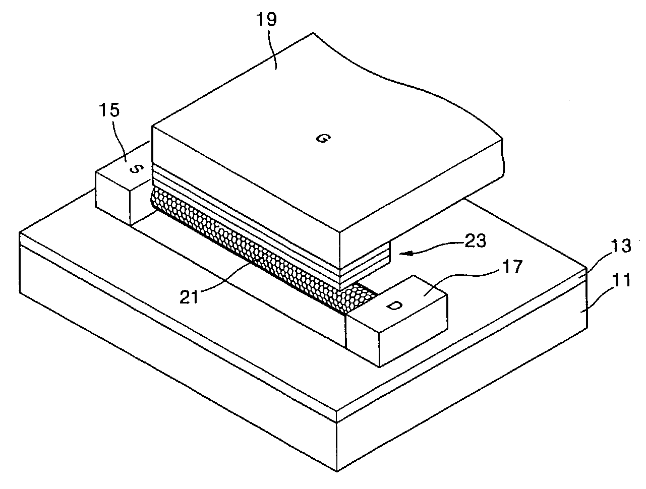
[0054]Referring to FIG. 1, a memory device according to an embodiment of the present invention includes a substrate 11, an insulating layer 13 deposited on the substrate 11, a source electrode 15 and a drain electrode 17 which are made of metal and separated by a predetermined distance from each other on the insulating layer 13, a carbon nanotube 21 which connects the source electrode 15 to the drain electrode 17 and serves as an electron moving channel, a memory cell 23 which contacts the carbon nanotube 21 and stores charges of electrons (or holes), and a gate electrode 19 which contacts the memory cell 23 and controls the movement of the electrons.

[0055]In FIG. 1, the source and drain electrodes 15 and 17 are installed on the subst...


PUM


Abstract

A fast, reliable, highly integrated memory device formed of a carbon nanotube memory device and a method for forming the same, in which the carbon nanotube memory device includes a substrate, a source electrode, a drain electrode, a carbon nanotube having high electrical and thermal conductivity, a memory cell having excellent charge storage capability, and a gate electrode. The source electrode and drain electrode are arranged with a predetermined interval between them on the substrate and are subjected to a voltage. The carbon nanotube connects the source electrode to the drain electrode and serves as a channel for charge movement. The memory cell is located over the carbon nanotube and stores charges from the carbon nanotube. The gate electrode is formed in contact with the upper surface of the memory cell and controls the amount of charge flowing from the carbon nanotube into the memory cell.

Description

BACKGROUND OF THE INVENTION[0001]1. Field of the Invention[0002]The present invention relates to a memory device and a method of fabricating the same. More particularly, the present invention relates to a memory device including a carbon nanotube that serves as a charge moving channel and a method of fabricating the memory device.[0003]2. Description of the Related Art[0004]Semiconductor memory devices fundamentally include a capacitor that preserves stored charges and a transistor that serves as a switch for securing a path of current necessary to write data to or read data from the capacitor.[0005]To allow a high current to flow in a transistor, the transistor must have a high transconductance (gin). Hence, metal oxide field effect transistors (MOSFETs) having a high transconductance have been commonly used as switching devices of semiconductor memory devices.[0006]MOSFETs basically include gate electrodes made of doped polycrystalline silicon and source and drain electrodes made ...

Claims


Application Information

Patent Timeline
IPC IPC(8): H01B7/08H01L35/24B82B1/00B82B3/00G11C13/02H01L21/8247H01L27/115H01L29/06H01L29/788H01L29/792
CPCB82Y10/00G11C13/025Y10S977/943G11C2213/17
Inventor CHOI, WON-BONGYOO, IN-KYEONGCHU, JAE-UK
Owner SAMSUNG ELECTRONICS CO LTD
Why Eureka
Try Eureka