Semiconductor device and manufacturing method thereof

a technology of semiconductor devices and silicide layers, which is applied in the direction of semiconductor devices, semiconductor/solid-state device details, electrical apparatus, etc., can solve the problems of increasing device power consumption, and achieve the effect of preventing the metal silicide layer in the underlying part and increasing the power consumption of the semiconductor devi

Active Publication Date: 2011-05-03
RENESAS ELECTRONICS CORP
View PDF3 Cites 4 Cited by
  • Summary
  • Abstract
  • Description
  • Claims
  • Application Information

AI Technical Summary

Benefits of technology

[0006]The present invention has been completed in view of the foregoing problem. It is an object of the present invention to provide a semiconductor device having a metal silicide layer, which can suppress the malfunction and the increase in power consumption of the device, and a manufacturing method thereof.
[0014]Under such circumstances, the present inventors found out the following: by performing a heat treatment after dry etching with no silicon depletion layer present, it is possible to suppress the increase in leak current. This has led to the completion of the present invention.
[0016]With the semiconductor device in accordance with this embodiment, the silicon depletion layer formed immediately under each contact hole is etched, and removed. As a result, a recess Part is formed in the surface of the metal silicide layer. For this reason, the silicon depletion layer will not further consume the silicon contained in the semiconductor substrate. In other words, it is possible to prevent the metal silicide layer in the underlying part of the contact hole from growing in the heat treatment after dry etching. This can prevent the malfunction and the increase in power consumption of the semiconductor device due to PN junction breakage.

Problems solved by technology

The present inventors have, for the first time, revealed the following problem: when contact holes are formed in an insulation film in order to form electrodes / wires to be in contact with the silicide layer, the leak current increases, which unfavorably causes the malfunction and the increase in power consumption of the device.

Method used


Image

  • Semiconductor device and manufacturing method thereof
  • Semiconductor device and manufacturing method thereof
  • Semiconductor device and manufacturing method thereof

Examples


embodiment 1

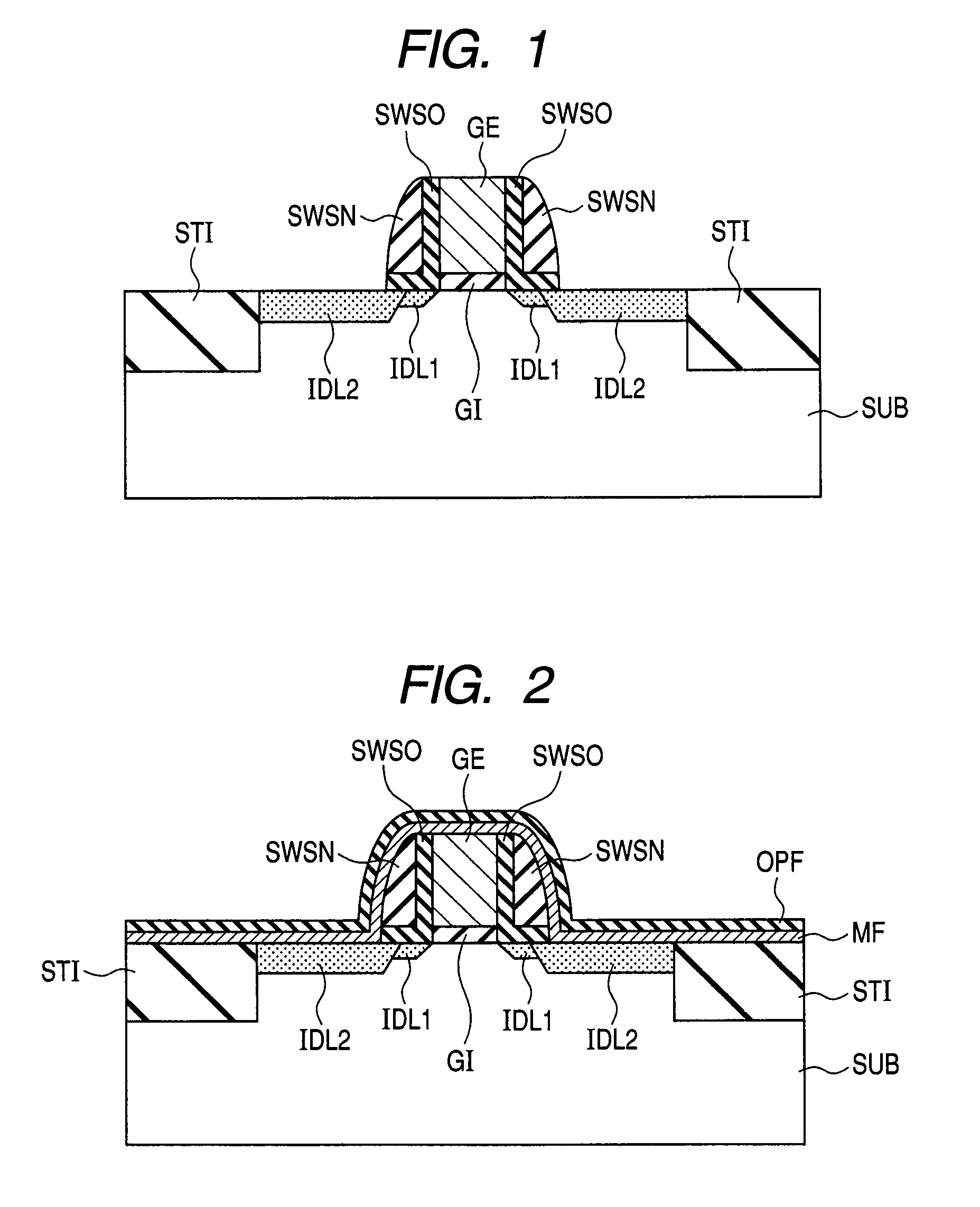
[0030]FIGS. 1 to 8 are schematic views for illustrating respective steps of a manufacturing method of a semiconductor device in accordance with Embodiment 1 of the present invention. By reference to FIGS. 1 to 8, the semiconductor device and the manufacturing method thereof of Embodiment 1 will be described.

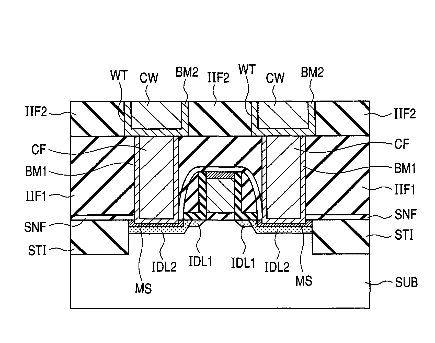
[0031]As shown in FIG. 1, in a region defined by an element isolation insulation film STI of a semiconductor substrate SUB which is a silicon (Si) substrate, a gate electrode GE including polysilicon is formed with a gate insulation film GI interposed therebetween. The gate electrode GE can be formed with a height of, for example, 100 nm. Over the main surface of the semiconductor substrate SUB, a first impurity diffusion layer IDL1 formed by ion implantation is formed with the gate electrode GE as a mask.

[0032]At the side surface of the gate electrode GE, a sidewall spacer is formed. The sidewall spacer is formed by lamination of a silicon oxide film SWSO and a silicon nitride f...

embodiment 2

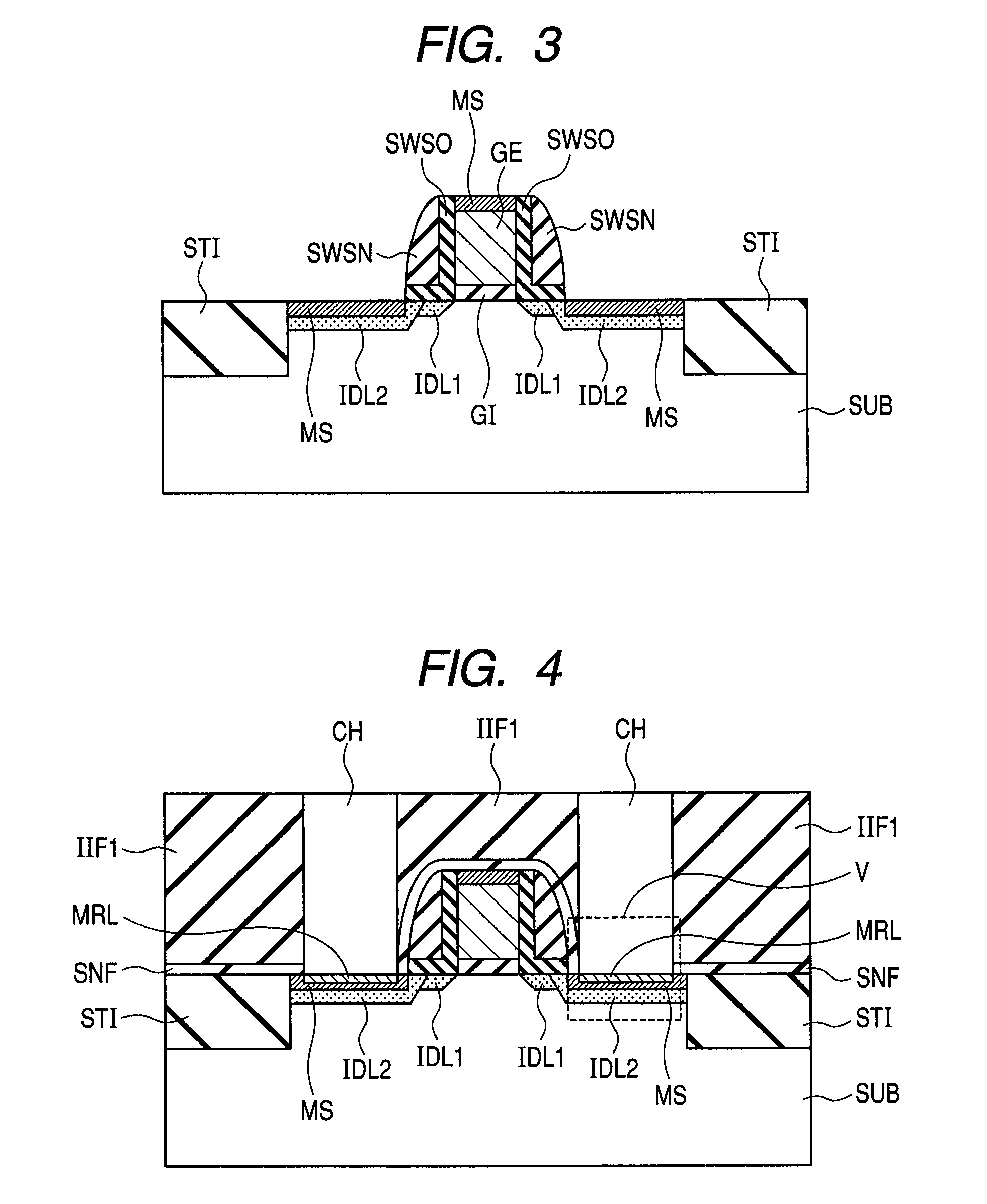
[0055]As described in Embodiment 1, upon removal of the metal-rich layer MRL which is the silicon depletion metal silicide immediately under the contact hole CH, the portion of the metal silicide MS in the underlying part of the contact hole CH is reduced in film thickness. When the metal silicide MS is reduced in film thickness, the metal silicide MS may agglomerate by the heat treatment in the subsequent semiconductor manufacturing step. In other words, the metal silicide MS may grow in islands (balls) to be an ununiform or discontinuous film.

[0056]When the metal silicide MS agglomerates, the contact resistance between the contact plug and the source / drain regions formed over the semiconductor substrate increases, and the driving current of the transistor decreases. Thus, in this embodiment, agglomeration due to the reduction of the film thickness of the metal silicide MS immediately under the contact hole CH is prevented.

[0057]FIG. 9 is a schematic view showing a step of a manufa...

embodiment 3

[0063]In Embodiments 1 and 2, a description was given to the technology of suppressing the abnormal growth of the portion of the metal silicide MS in the underlying part of the contact hole CH by removing the Si-depleted metal silicide layer (metal-rich layer MRL). In this embodiment, there is provided a method for suppressing the Si depletion of the portion of the metal silicide MS in the underlying part of the contact hole CH. In other words, in this embodiment, there is provided a technology for preventing the formation of the metal-rich layer MRL in the manufacturing method of the semiconductor device.

[0064]FIGS. 10 to 12 are schematic views for illustrating respective steps of a manufacturing method of a semiconductor device in accordance with Embodiment 3. After formation of the metal silicide MS by the steps shown in FIGS. 1 to 3, as shown in FIG. 10, a silicon oxide layer SOL as a protective insulation film is thinly stacked selectively over the metal silicide MS. The silico...


PUM

PropertyMeasurementUnit
temperatureaaaaaaaaaa
heightaaaaaaaaaa
thicknessaaaaaaaaaa

Abstract

There is provided a semiconductor device having a metal silicide layer which can suppress the malfunction and the increase in power consumption of the device. The semiconductor device has a semiconductor substrate containing silicon and having a main surface, first and second impurity diffusion layers formed in the main surface of the semiconductor substrate, a metal silicide formed over the second impurity diffusion layer, and a silicon nitride film and a first interlayer insulation film sequentially stacked over the metal silicide. In the semiconductor device, a contact hole penetrating through the silicon nitride film and the first interlayer insulation film, and reaching the surface of the metal silicide is formed. The thickness of a portion of the metal silicide situated immediately under the contact hole is smaller than the thickness of a portion of the metal silicide situated around the contact hole.

Description

CROSS-REFERENCE TO RELATED APPLICATIONS[0001]The disclosure of Japanese Patent Application No. 2008-130740 filed on May 19, 2008 including the specification, drawings and abstract is incorporated herein by reference in its entirety.BACKGROUND OF THE INVENTION[0002]The present invention relates to a semiconductor device and a manufacturing method thereof. More particularly, it relates to a semiconductor device having a metal silicide layer, and a manufacturing method thereof.[0003]In order to achieve a lower resistance of a semiconductor device, there has been generally employed a method in which a silicide is formed between the wiring material and the substrate. A conventional semiconductor device having a metal silicide layer is proposed in, for example, Patent Document 1.[0004][Patent Document 1]Japanese Unexamined Patent Publication No. Hei 09 (1997)-283462SUMMARY OF THE INVENTION[0005]The present inventors have, for the first time, revealed the following problem: when contact ho...

Claims


Application Information

Patent Timeline
Patent Type & Authority Patents(United States)
IPC IPC(8): H01L29/76
CPCH01L21/28518H01L23/485H01L2924/0002H01L2924/00
Inventor TSUTSUMI, TOSHIAKIOKUDAIRA, TOMONORIKASHIHARA, KEIICHIROYAMAGUCHI, TADASHI
Owner RENESAS ELECTRONICS CORP
Why Eureka
Try Eureka