SOI stacked dram logic

a logic and stacking technology, applied in semiconductor/solid-state device testing/measurement, semiconductor device details, semiconductor/solid-state device testing/measurement, etc., can solve the problem of incompatibility of soi transistors and trench capacitors, large chip area and other issues, to achieve the effect of avoiding the formation of memory cells

Inactive Publication Date: 2002-03-28
IBM CORP
View PDF0 Cites 217 Cited by
  • Summary
  • Abstract
  • Description
  • Claims
  • Application Information

AI Technical Summary

Problems solved by technology

However, the support circuitry requires substantial chip area which is thus not available for formation of memory cells.
However, SOI transistors and trench capacitors are not compatible and cannot be easily integrated on the same chip.
Further, the active device layer of SOI wafers is too thin to provide adequate capacitance at currently feasible minimum lithographic feature sizes and forming a trench through the insulator of an SOI wafer or chip would compromise the electrical isolation thereof.
Moreover, the thermal budget required to form trench capacitors and node interconnections greatly exceeds the desired heat budget for forming high speed, low voltage logic switching devices in SOI.
Another problem involving on-chip capacitances required in increasing numbers of types of integrated circuits is the decoupling capacitance which is required in logic circuits operating at low voltage and clock frequencies greater than about 400 MHz to prevent unacceptable levels of switching noise (relative to the operating voltage) from being propagated through power connections.
The intrachip area required for a planar capacitor is so large that multiple power supplies to reduce power/performance trade-offs cannot be included on the chip since the voltage regulators cannot b...

Method used


Image

  • SOI stacked dram logic
  • SOI stacked dram logic
  • SOI stacked dram logic

Examples


Embodiment Construction

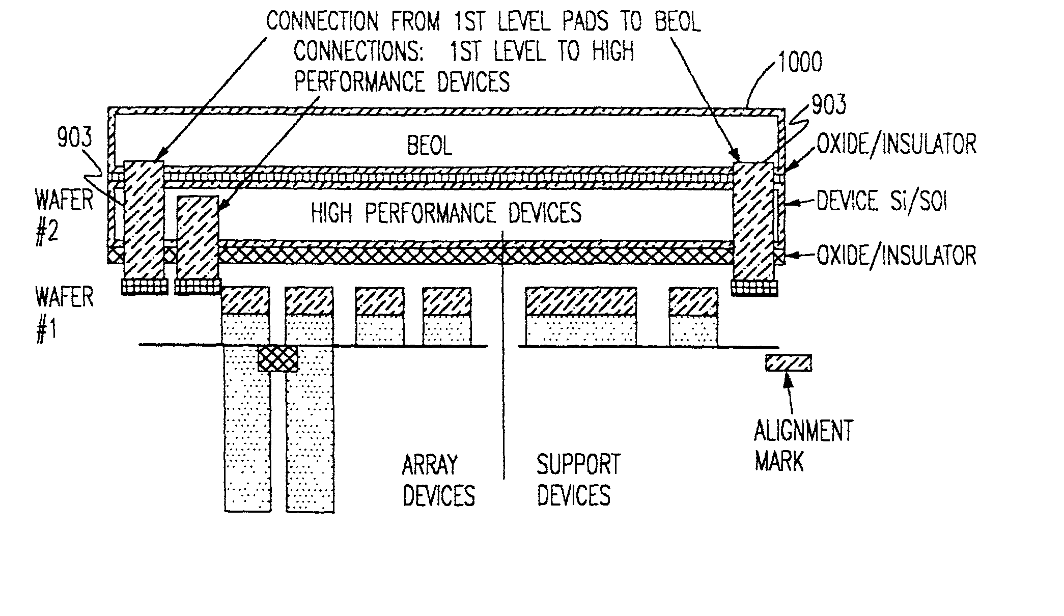
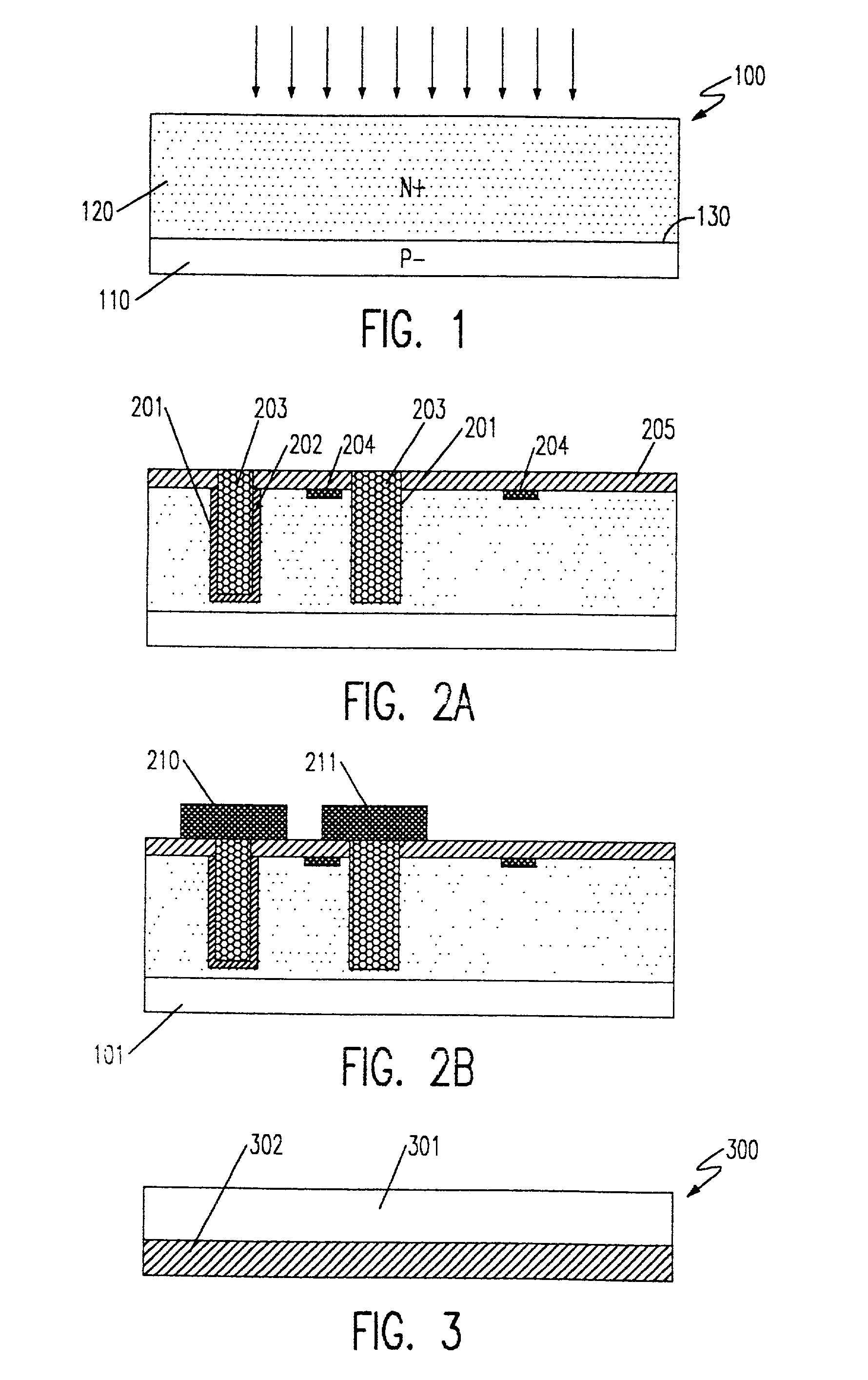
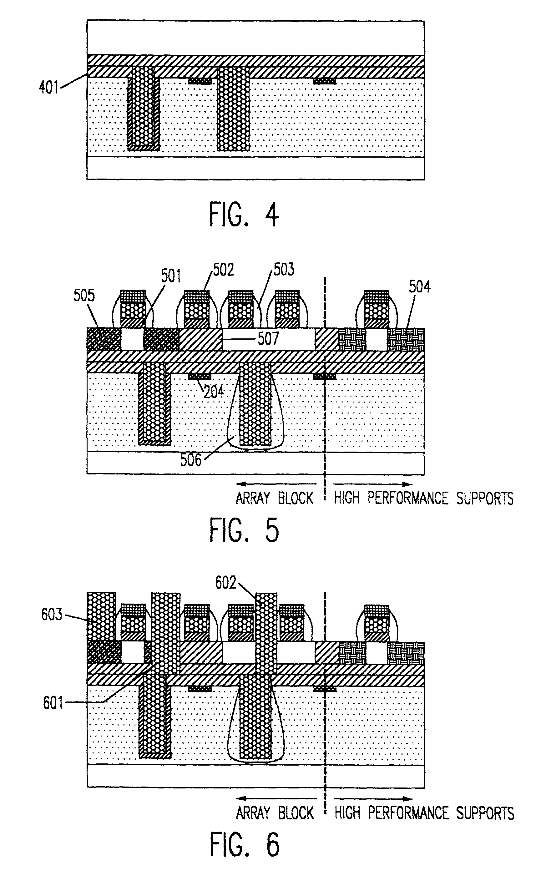
[0026] Referring now to the drawings, and more particularly to FIG. 1, there is shown, in cross-sectional view, a bulk silicon wafer 100, preferably of the p- type. However, it should be understood that the conductivity types of impurities are not important to the principles of the invention or the types of circuit elements integrated therein to which the invention may be applied. That is, while the invention clearly has particular applicability to dynamic memories with respect to which it will be explained and for which the illustrated conductivities are preferred, the invention is more generally directed to the formation of composite, layered, chips with optimally short and reliably formed interconnections therebetween which are lithographically defined at pitches comparable to intra chip connections while incorporating incompatible technologies.

[0027] For purposes of forming a dynamic memory array, a deep n+ implantation is performed to create a thick conductive plate layer 120 w...


PUM


Abstract

A composite, layered, integrated circuit formed by bonding of insulator layers on wafers provides for combination of otherwise incompatible technologies such as trench capacitor DRAM arrays and high performance, low power, low voltage silicon on insulator (SOI) switching transistors and short signal propagation paths between devices formed on respective wafer layers of a chip. In preferred embodiments, an SOI wafer is formed by hydrophilic bonding of a wafer over an integrated circuit device and then cleaving a layer of the second wafer away using implanted hydrogen and low temperature heat treatment. Further wafers of various structures and compositions may be bonded thereover and connections between circuit elements and connection pads in respective wafers made using short vias that provide fast signal propagation as well as providing more numerous connections than can be provided on chip edges.

Description

[0001] 1. Field of the Invention[0002] The present invention generally relates to semiconductor integrated circuits and, more particularly, to high capacity dynamic random access memories including high performance transistors in support circuitry thereof and other types of devices having differing circuit element requirements and to testing and burn-in thereof.[0003] 2. Description of the Prior Art[0004] As the processing power of microprocessors has increased and cycle times reduced, higher capacity memories with more rapid access time have been demanded. Accordingly, dynamic memories have been developed with storage cells requiring reduced area or footprint such that memory chips having a capacity of a gigabit or more can be foreseen. Such storage cells are often formed by lining trenches in a chip of doped semiconductor with an insulator and filling the remainder of the trench with doped polysilicon to form an array of capacitors having a common electrode formed by the chip. A s...

Claims


Application Information

Patent Timeline
IPC IPC(8): H01L21/768H01L21/8242H01L23/48H01L23/58H01L27/108H01L27/12
CPCH01L21/76838H01L21/76895H01L2924/0002H01L22/32H01L23/481H01L27/10832H01L27/10867H01L27/1203Y10S977/90Y10S977/779Y10S977/712Y10S977/721Y10S977/94H01L2924/00H01L23/535H10B12/373H10B12/0385
Inventor DIVAKAUNI, RAMACHANDRAHAKEY, MARK C.MA, WILLIAM H-L.MANDCLMAN, JACK A.TONTI, WILLIAM R.
Owner IBM CORP
Why Eureka
Try Eureka