Method for manufacturing semiconductor device

a manufacturing method and semiconductor technology, applied in the direction of semiconductor devices, printing, fastener tools, etc., can solve the problems of complex process step for removing materials, difficult to additionally remove silicon oxide films or interconnects in the process for etching the wafer, so as to reduce the processing width of the dicing process for the semiconductor wafer

Inactive Publication Date: 2006-09-14
NEC ELECTRONICS CORP
View PDF6 Cites 201 Cited by
  • Summary
  • Abstract
  • Description
  • Claims
  • Application Information

AI Technical Summary

Benefits of technology

[0012] According to the method, the protective film is provided on the device-forming surface, and the protective film is irradiated with a laser beam to form the trenched portion. Consequently, the trenched portion can be stably provided in a certain location. In addition, the irradiation of the protective film with the laser beam allows conducting a dicing process while providing a protection to the surface of the semiconductor substrate. Further, when an interposing layer is presented between the semiconductor substrate and the protective film, the trenched portion extending through the interposing layer can be simply and surely provided by irradiating with a laser beam to provide a trenched portion extending to the inside of the semiconductor substrate. Further, since the irradiation with the laser beam is employed for forming the trenched portion, width of the formed trenched portion can be reduced, as compared with the conventional dicing process that employs a dicing saw. Moreover, since portions of the semiconductor substrate are removed selectively in depth direction after it is irradiated with a laser beam to provide the trenched portion that extends to the inside of the semiconductor substrate, rate of the processing for providing the trenched portion can be improved, while the reduced width of the trenched portion is ensured.
[0013] As such, according to the method of the present invention, the processing width in the dicing process can be reduced, while providing the protection to the device-forming surface of the semiconductor substrate. Thus, degree of integration in the device-forming region provided in one piece of the semiconductor substrate can be enhanced, and a production yield for producing the semiconductor device by dicing the semiconductor substrate along the periphery of the device-forming region can be improved.
[0016] As described above, according to the present invention, the processing width of the dicing process for the semiconductor wafer can be reduced by providing the protective film on the device-forming surface, irradiating the protective film with a laser beam to provide a trenched portion extending in the inside of the semiconductor substrate from the protective film, and thereafter, selectively removing the semiconductor substrate from a bottom of the trenched portion in depth direction, and dividing the semiconductor substrate along portions where the trenched portion is provided into respective pieces of the semiconductor substrate.

Problems solved by technology

Therefore, when an oxide film or an interconnect is provided in a region to be removed via a dicing on a device formation surface (circuit surface) on the wafer, a complicated process step for removing materials except silicon conducted with the etch process for the wafer is required.
However, when a silicon oxide film or an interconnect are in the dicing region, it is difficult to additionally remove the silicon oxide film or the interconnects in the process for etching the wafer.
Therefore, the aforementioned problem of “when a silicon oxide film or an interconnect are in the dicing region, it is difficult to additionally remove the silicon oxide film or the interconnects in the process for etching the wafer” existing in the technology described in Japanese Patent Laid-Open No. 2003-179,005 has not been solved.

Method used


Image

  • Method for manufacturing semiconductor device
  • Method for manufacturing semiconductor device
  • Method for manufacturing semiconductor device

Examples


first embodiment

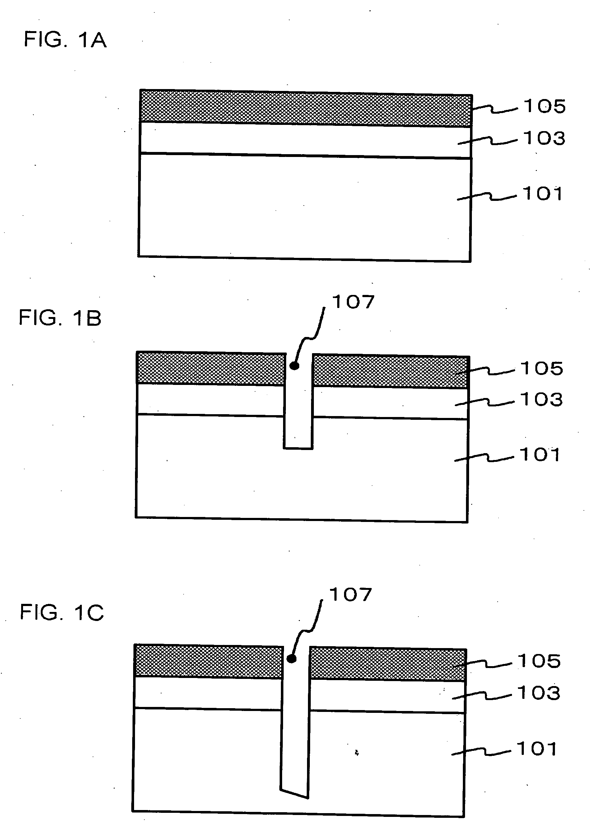
[0032]FIG. 1A to FIG. 1C, FIG. 2A and FIG. 2B are cross-sectional views, illustrating a process for manufacturing a semiconductor device of the present embodiment. FIG. 3 is a plan view, illustrating a configuration of the semiconductor wafer in a status of preliminary step to the status of FIG. 1A. FIG. 4 is a cross-sectional view illustrating a configuration of the semiconductor device obtained by procedures shown in FIG. 3, FIG. 1A to FIG. 1C, FIG. 2A and FIG. 2B. FIG. 4 represents the view corresponds to a cross-section along line A-A′ of FIG. 3.

[0033] First of all, the configuration of the semiconductor device according to the present embodiment will be described in reference to FIG. 3 and FIG. 4. A semiconductor device 100 shown in FIG. 3 and FIG. 4 is configured that a silicon wafer 101 is divided by dicing along dicing lines 120, and an interconnect layer 103 is provided on each of the divided silicon wafer 101. The interconnect layer 103 includes an insulating film (not sh...

second embodiment

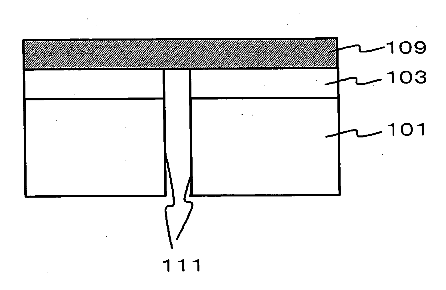
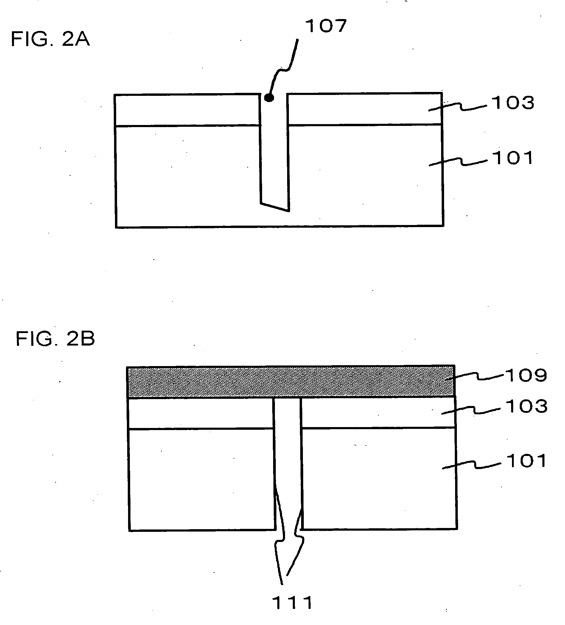
[0092] In first embodiment, after the dry etching operation in step 103 (FIG. 1C), the protective film 105 is stripped (FIG. 2A), and the back surface grinding is conducted for the silicon wafer 101 to obtain a plurality of semiconductor devices 100 (FIG. 2B). In the present embodiment, the dry etch process for the silicon wafer 101 is further continued, in place of the back surface polishing, to divide the silicon wafer 101 into a plurality of semiconductor devices 100. More specifically, the operation for dividing the silicon wafer 101 into pieces in step 104 includes an operation for further removing the silicon wafer 101 in depth direction from the bottom of the trenched portion 107 via an etch process. The operation for removing the protective film 105 in step 106 is conducted after the after the operation for dividing the wafer in step 104.

[0093]FIG. 7A to FIG. 7C and FIG. 8A to FIG. 8C are cross-sectional views, illustrating a process for manufacturing a semiconductor device...

third embodiment

[0097] In the present embodiment, a pad electrode and a metal-plated bump are further provided on the interconnect layer 103, and thereafter, a dicing process is conducted. In this case, a plurality of semiconductor devices can similarly be obtained from one piece of the silicon wafer 101 by employing the process described in the above embodiments.

[0098]FIG. 9 is a cross-sectional view, illustrating a configuration of a semiconductor device of the present embodiment. A semiconductor device 130 shown in FIG. 9 further includes the following members, in addition to the configuration of the semiconductor device 100 shown in FIG. 1. More specifically, an insulating interlayer 131 is provided on an interconnect layer 103, and an interconnect 133 is buried within the insulating interlayer 131. Materials of the interconnect 133 may include, for example, conductive materials such as metals such as Cu or Al and the like. In addition, an electroconductive electrode pad 135 is provided on the...


PUM


Abstract

A method of dicing a semiconductor wafer includes providing an interconnect layer providing a protective film on the interconnect layer on the side of a device-forming surface of a silicon wafer, irradiating the protective film with a laser beam to provide a trenched portion that extends through the interconnect layer from the protective film and reaches to an inside of the silicon wafer, removing a portion of the silicon wafer selectively in a depth direction from a bottom of the trenched portion, after irradiating with the laser beam to provide the trenched portion and dividing the silicon wafer along the portion where the trenched portion is provided into respective pieces of the silicon wafer, after removing a portion of the silicon wafer 101 selectively in the depth direction.

Description

[0001] This application is based on Japanese patent application No. 2005-067,626, the content of which is incorporated hereinto by reference. BACKGROUND [0002] 1. Technical Field [0003] The present invention relates to a method for manufacturing a semiconductor device, and particularly relates to method for isolating a plurality of semiconductor devices formed thereon into individual devices. [0004] 2. Related Art [0005] A dicing process and an etch process have conventionally been employed as processes for dividing a plurality of semiconductor devices formed on a wafer into individual devices. Such type of technology is described in Japanese Patent Laid-Open No. 2003-179,005 and Japanese Patent Laid-Open No. 2004-55,684. [0006] In the method disclosed in Japanese Patent Laid-Open No. 2003-179,005, a half-cut-off is first formed by etching a dicing line from a side of a surface of a wafer having an electronic circuit formed thereon. A back grinding tape is adhered onto a front surfa...

Claims


Application Information

Patent Timeline
Patent Type & Authority Applications(United States)
IPC IPC(8): H01L21/00
CPCH01L21/78H01L2224/11B43M15/00Y10S411/921Y10S411/923
Inventor SOEJIMA, KOJI
Owner NEC ELECTRONICS CORP
Why Eureka
Try Eureka