Backside contact for touchchip

a touchchip and contact pad technology, applied in the direction of electrical equipment, semiconductor devices, semiconductor/solid-state device details, etc., can solve the problems of limiting the materials which may be used for passivation, increasing the size requirement of dies, and presenting other processing challenges

Inactive Publication Date: 2001-12-04
STMICROELECTRONICS SRL
View PDF12 Cites 216 Cited by
  • Summary
  • Abstract
  • Description
  • Claims
  • Application Information

AI Technical Summary

Problems solved by technology

Since die contact pads are generally formed using every metallization layer on the front side and are never formed over active devices, placement of the contact pads on the wafer's front side may increase the size requirement of the die.
For some types of integrated circuits, placement of die contact pads on the front side of the integrated ci

Method used


Image

  • Backside contact for touchchip
  • Backside contact for touchchip
  • Backside contact for touchchip

Examples


Embodiment Construction

The following description details the structure, application and features of the present invention, but it will be understood by those of skill in the art that the scope of the invention is defined only by the issued claims, and not by any description herein. The process steps and structures described below do not form a complete process flow for manufacturing integrated circuits. The present invention can be practiced in conjunction with integrated circuit fabrication techniques currently used in the art, and only so much of the commonly practiced process steps are included as are necessary for an understanding of the present invention. The figures representing cross-sections of portions of an integrated circuit during fabrication are not drawn to scale, but instead are drawn so as to illustrate the important features of the invention.

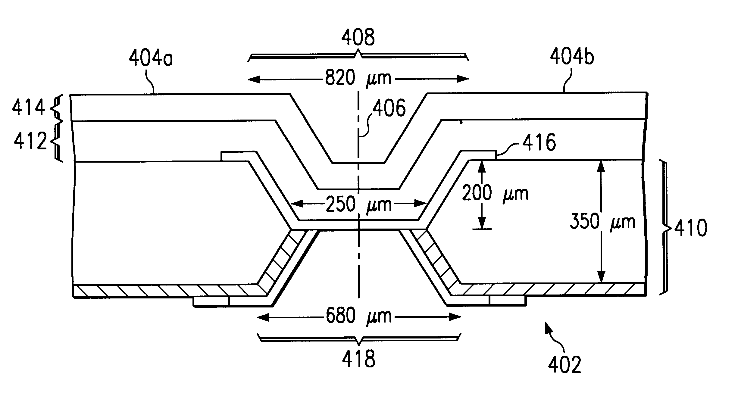
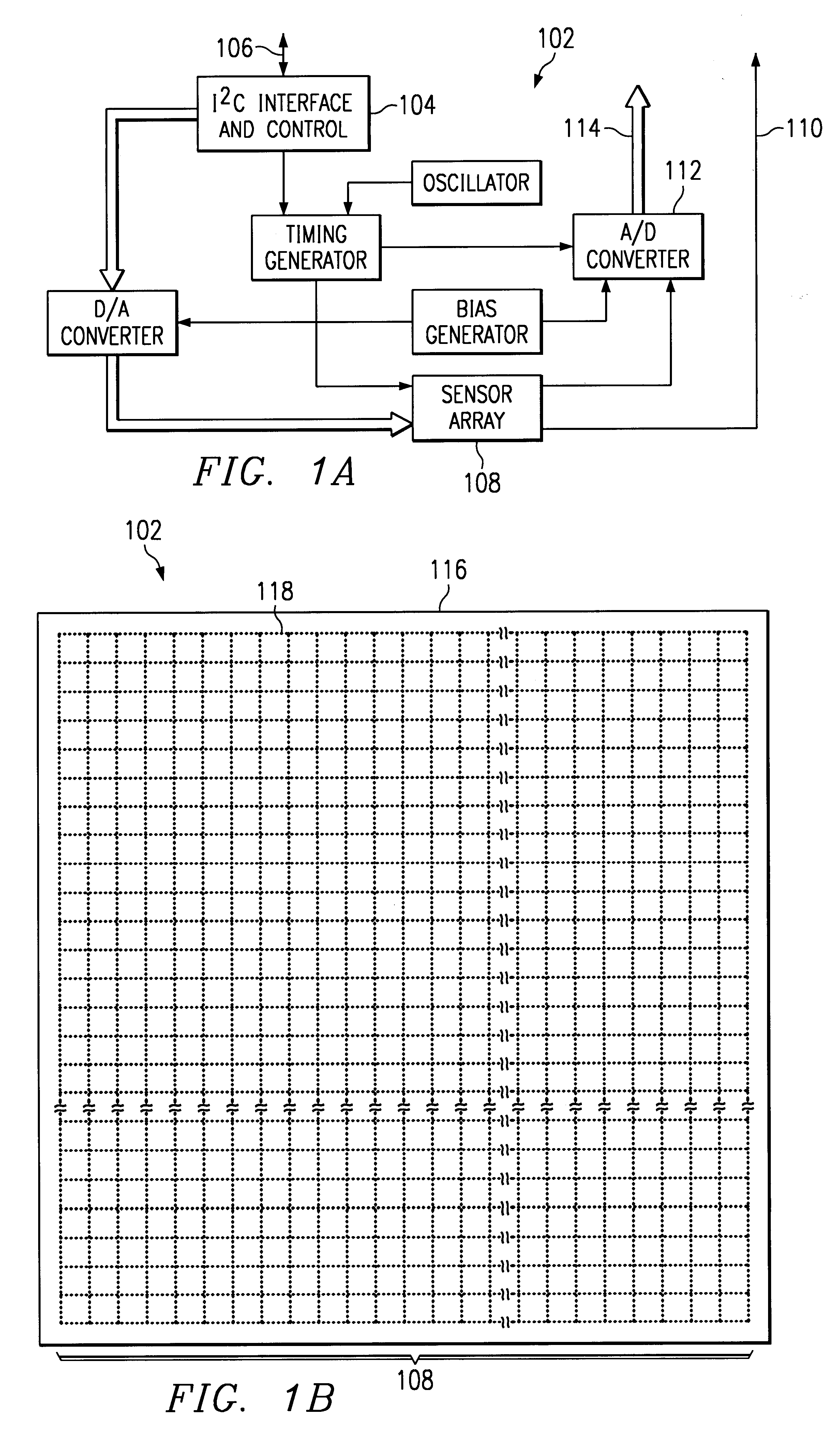
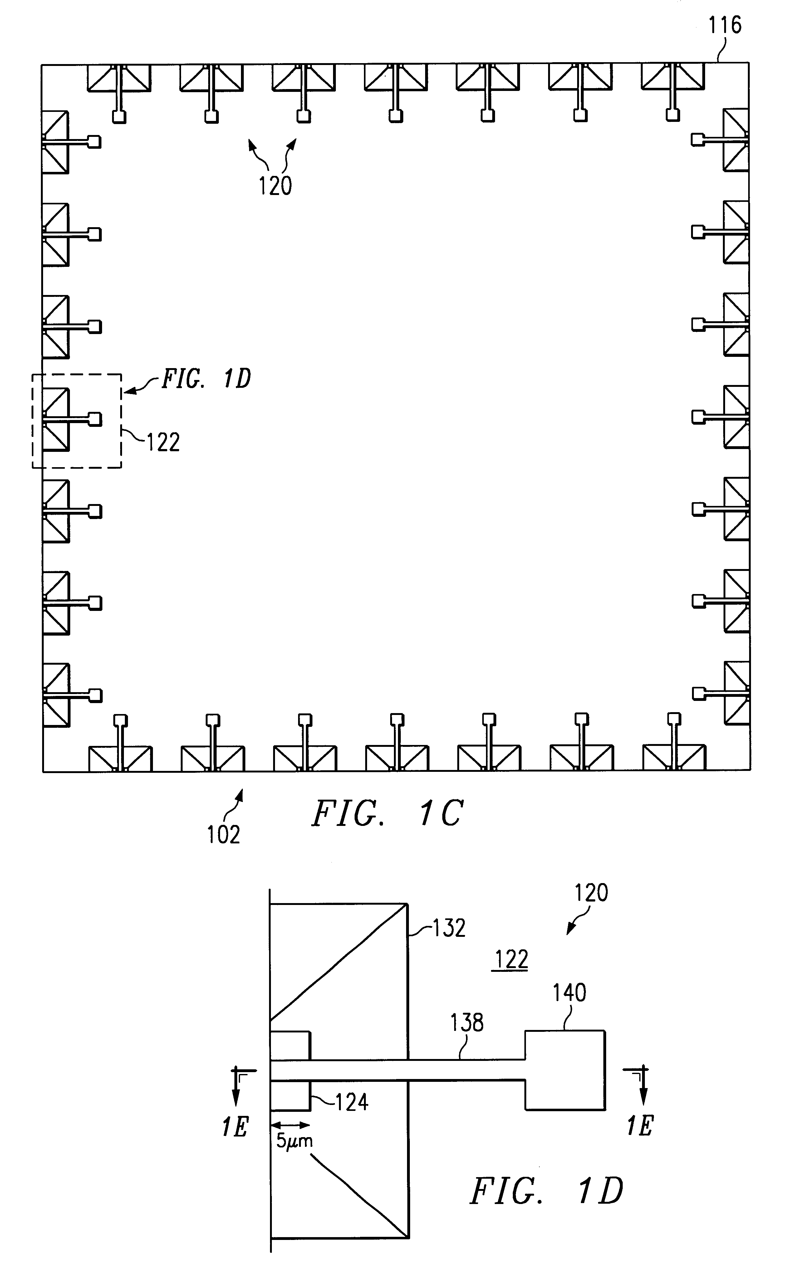
With reference now to the figures, and in particular with reference to FIGS. 1A through 1E, various views of a sensor circuit employing backside cont...


PUM


Abstract

A contact is formed within an active region of a substrate at the edge of a die, preferably within the first metallization level in the active region of the substrate. An opening having sloped sidewalls is then etched into the back side of the substrate, exposing a portion of the active region contact. An interconnect is formed on the opening sidewall to connect the active region contact with a die contact pad on the backside surface of the substrate. The active region contact preferably spans a boundary between two die, with the opening preferably etched across the boundary to permit inter-connects on opposing sidewalls of the opening to each contact the active region contact within different die, connecting the active region contact to die contact pads on different dice. The dice are then separated along the boundary, through the active region contact which becomes two separate active region contacts. By forming a shared contact opening spanning two dice, the backside contact is formed around the die edge and the backside surface area necessary for the contact opening is minimized. The backside contact allows direct placement of the integrated circuit die on contacts within the packaging, such as a ball grid array, eliminating the need for wire bonds. The need for a pad etch through passivation material overlying active devices on the front side of the die is also eliminated, and no mask levels are added for the devices formed on the front side.

Description

1. Field of the InventionThe present invention relates generally to die contacts in integrated circuits, and more specifically to backside contact pads employed in lieu of conventional peripheral contact pads.2. Description of the Prior Art:Integrated circuits have conventionally employed contact pads on the "front" side of a wafer, or the side of a wafer on which devices are or were formed. The contacts pads, normally square-shaped and approximately 100 .mu.m on a side, are usually located around a peripheral portion of each die. Wires, typically gold, are then formed to connect each die contact pad to an appropriate pad in the packaging, which is generally electrically connected, in turn, to a pin.Since die contact pads are generally formed using every metallization layer on the front side and are never formed over active devices, placement of the contact pads on the wafer's front side may increase the size requirement of the die. If a large number of contact pads are required and...

Claims


Application Information

Patent Timeline
IPC IPC(8): H01L23/48
CPCH01L23/481H01L2224/05569H01L2224/02371H01L2224/0401H01L2224/131H01L2924/0002H01L2924/014H01L2224/05552
Inventor THOMAS, DANIELLE A.
Owner STMICROELECTRONICS SRL
Why Eureka
Try Eureka