Semiconductor integrated circuit device

a technology of integrated circuit and semiconductor, applied in the direction of logic circuit coupling/interface arrangement, pulse technique, instruments, etc., can solve the problems of increasing man-hours spent on circuit block arrangement design for that purpose, and the above-stated power saving technique cannot be applied, so as to achieve the effect of saving power consumption and being easy to generate and match

Active Publication Date: 2009-10-29
RENESAS ELECTRONICS CORP
View PDF5 Cites 5 Cited by
  • Summary
  • Abstract
  • Description
  • Claims
  • Application Information

AI Technical Summary

Benefits of technology

[0007]These configurations in which are arranged, apart from circuit blocks to perform the essential functions of the circuit, circuit blocks which prevent unfixed signals in the circuit block to which power supply has been cut off is prevented from being transmitted to the circuit block to which power is supplied, such as the wrapper and the micro I / O circuit, involve a problem of increased man-hours spent on the designing of circuit block arrangement for that purpose. Especially the configuration according to Patent Reference 2 involves a problem of requiring different ways of control to match four cases of power cut-off, as stated in paragraph 0020 of the specification, because where the micro I / O circuit has a level changing function, the earlier stage is supplied with the same source voltage as the sending-side circuit block and the later stage is supplied with the same source voltage as the receiving-side circuit block, with the consequence that one circuit block is supplied with a common source voltage to a different circuit block.
[0010]With a simple configuration, inputs at unfixed levels to a circuit block in an operating state can be prevented while saving power consumption by interrupting power supply to a standing-by circuit block. The control signal for the prevention of inputs at unfixed levels can be easily generated and matched with power cut-off control.

Problems solved by technology

Therefore, where a plurality of functions are mounted on a single semiconductor integrated circuit device as in a system LSI and there are both operating functional blocks and non-operating functional blocks, the above-stated technique of power saving by cutting off power supply to non-operating functional blocks cannot be applied.
These configurations in which are arranged, apart from circuit blocks to perform the essential functions of the circuit, circuit blocks which prevent unfixed signals in the circuit block to which power supply has been cut off is prevented from being transmitted to the circuit block to which power is supplied, such as the wrapper and the micro I / O circuit, involve a problem of increased man-hours spent on the designing of circuit block arrangement for that purpose.

Method used


Image

  • Semiconductor integrated circuit device
  • Semiconductor integrated circuit device
  • Semiconductor integrated circuit device

Examples


Embodiment Construction

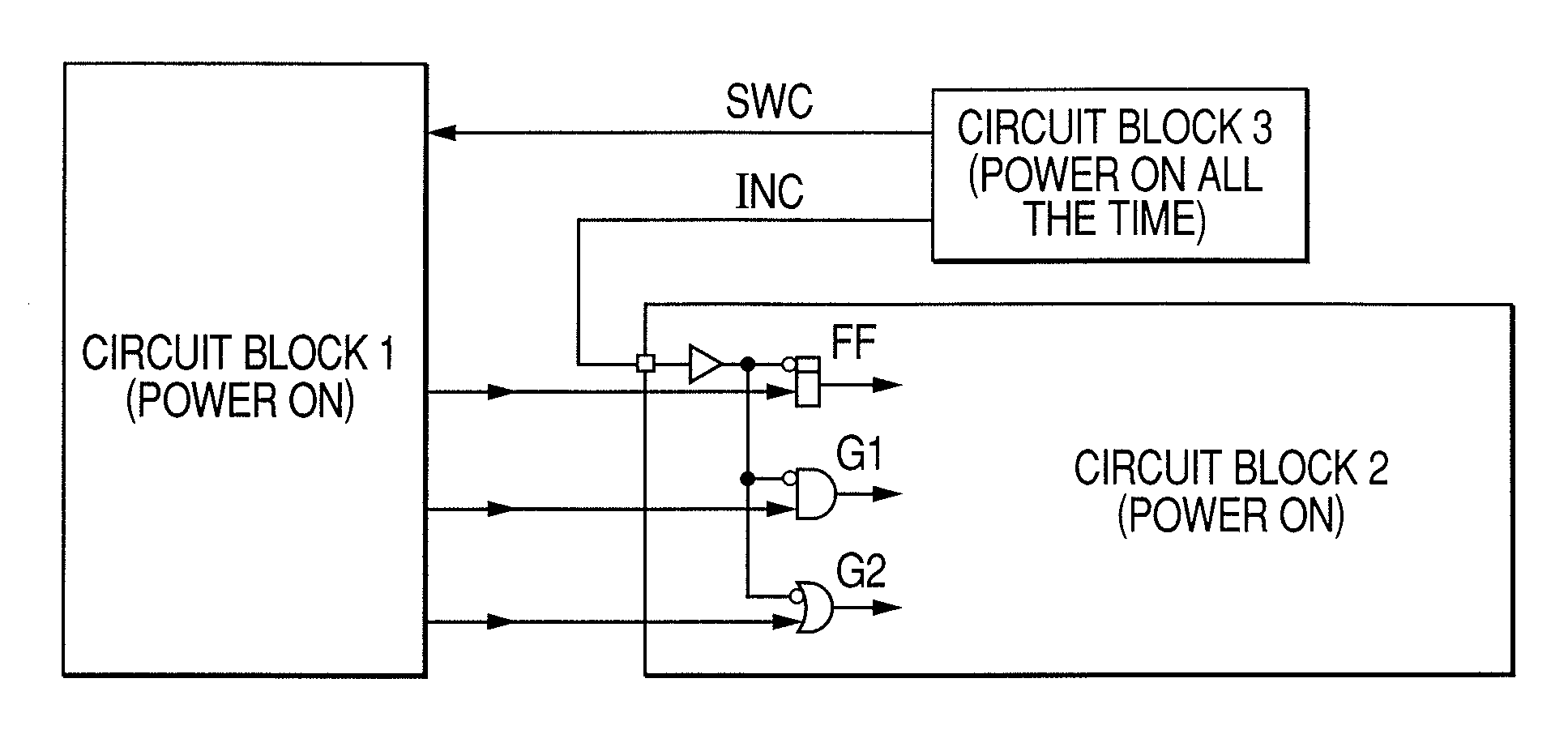
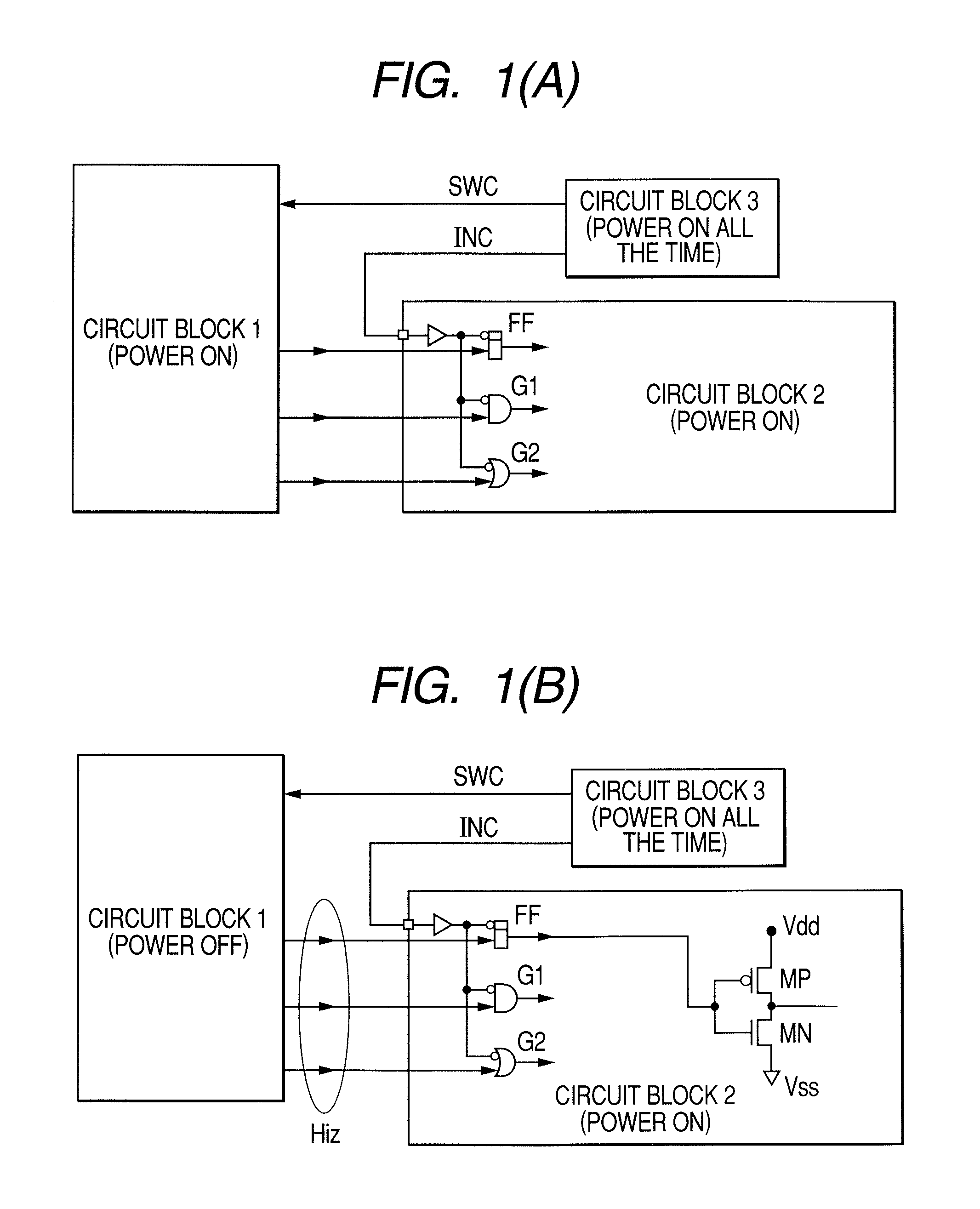
[0034]FIG. 1 show the configurations of the smallest unit of a semiconductor integrated circuit device, which is a preferred embodiment of the present invention. FIG. 1(A) shows one example of one type of operating state, and FIG. 1(B), one example of another type of operating state. The smallest unit of the semiconductor integrated circuit device of this embodiment consists of three circuit blocks. A circuit block 1, turned off in a standby state, is provided with a power switch. A circuit block 2 has a circuit portion which operates in response to a signal from the circuit block 1. The presence or absence of the function of turning off when standing by is irrelevant to the circuit block 2. The circuit block 1 is provided with a circuit block 3 which generates a control signal SWC for power supply control and a control signal INC for preventing propagation of unfixed levels from a circuit block to which power supply is turned off. Power supply to this circuit block 3 is on all the ...


PUM


Abstract

A semiconductor integrated circuit device enhanced in design efficiency while achieving multi-functionalization and power saving is to be provided. The semiconductor integrated circuit device has first through third circuit blocks, and is placed in a first power supply state in which the operation of internal circuits in the first circuit block is guaranteed in accordance with an instruction from the third circuit block or a second power supply state in which the operation of the internal circuits is not guaranteed. The second circuit block has an input unit which receives signals supplied from the first circuit block, and the input unit of the second circuit block has an input circuit which, in accordance with a control signal sent from said third circuit block to said second circuit block, causes a specific signal level to be maintained in compliance with the operating voltage of the second circuit block irrespective of the signal supplied from the first circuit block when the third circuit block instructs the second power supply state to the first circuit block.

Description

CROSS REFERENCE TO RELATED APPLICATION[0001]This application is a continuation of U.S. application Ser. No. 11 / 109,660, filed Apr. 20, 2005, and which application claims priority from Japanese patent application No. 2004-124683 filed on Apr. 20, 2004, the contents of which are hereby incorporated by reference into this application.BACKGROUND OF THE INVENTION[0002]The present invention relates to a semiconductor integrated circuit device, and more particularly to a technique that can be effectively applied to, for instance, a system large scale integrated circuit (LSI) in which each of a plurality of functional modules is divided into circuit blocks and power supplied is turned on or off according to the operation or non-operation of each functional module.[0003]There is Japanese Unexamined Patent Publication No. 2002-026711, which discloses a configuration in which the circuit is divided into a circuit block consisting of a MOSFET having a low threshold voltage and a circuit block c...

Claims


Application Information

Patent Timeline
Patent Type & Authority Applications(United States)
IPC IPC(8): G05F1/10G05F3/02H01L21/822G11C5/00G11C5/14H01L27/04H03K19/00H03K19/0175
CPCG11C5/147
Inventor AZUMA, YURIYASU, YOSHIHIKOIGARASHI, YASUTOKURAISHI, TAKASHIYANAGISAWA, KAZUMASA
Owner RENESAS ELECTRONICS CORP
Why Eureka
Try Eureka