

Nonvolatile storage device and method for manufacturing same
a storage device and non-volatile technology, applied in the direction of semiconductor devices, diodes, electrical apparatus, etc., can solve the problems of inability to give, difficult to draw out the peripheral circuit, and inability to meet the requirements of the peripheral circuit,
- Summary
- Abstract
- Description
- Claims
- Application Information
AI Technical Summary
Problems solved by technology
Method used
Image

Examples
first embodiment
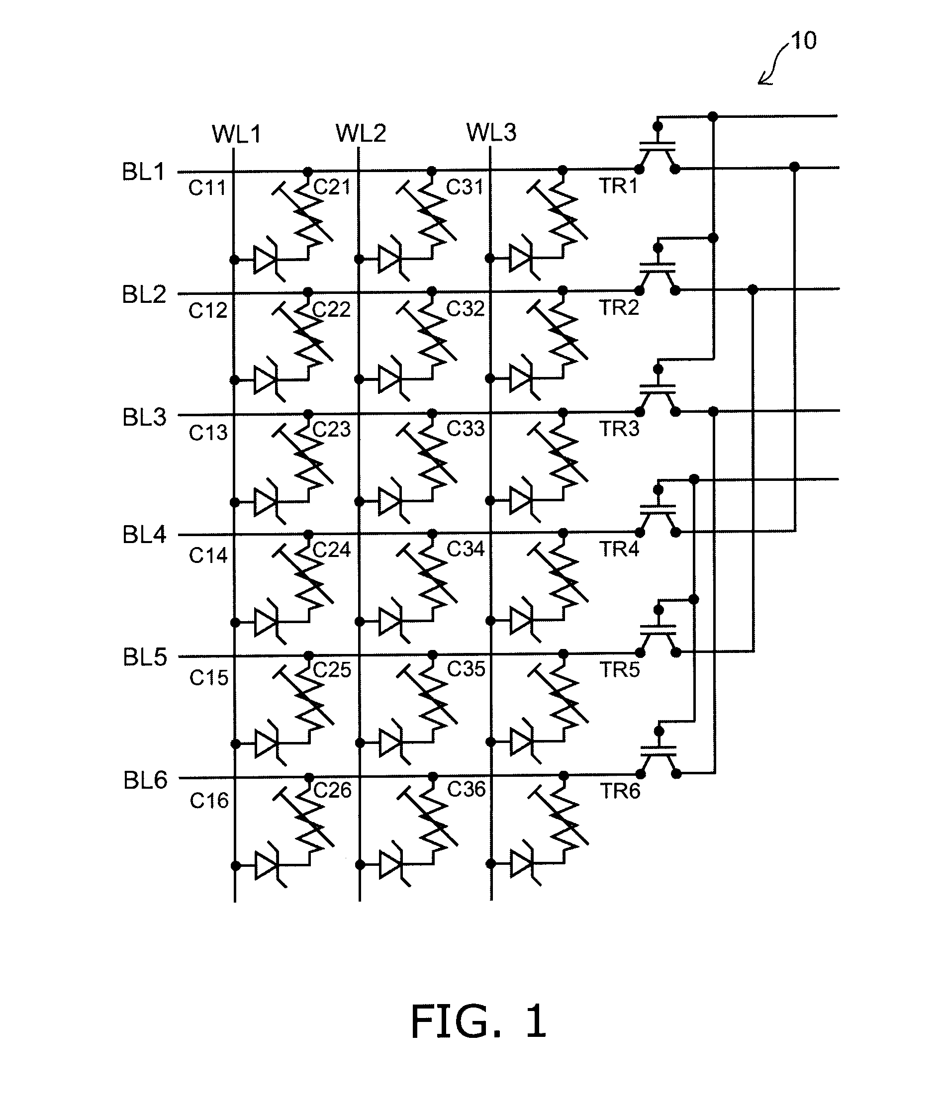
[0030]FIG. 1 is a circuit configuration diagram illustrating a structure of a nonvolatile storage device according to a first embodiment of the present invention.
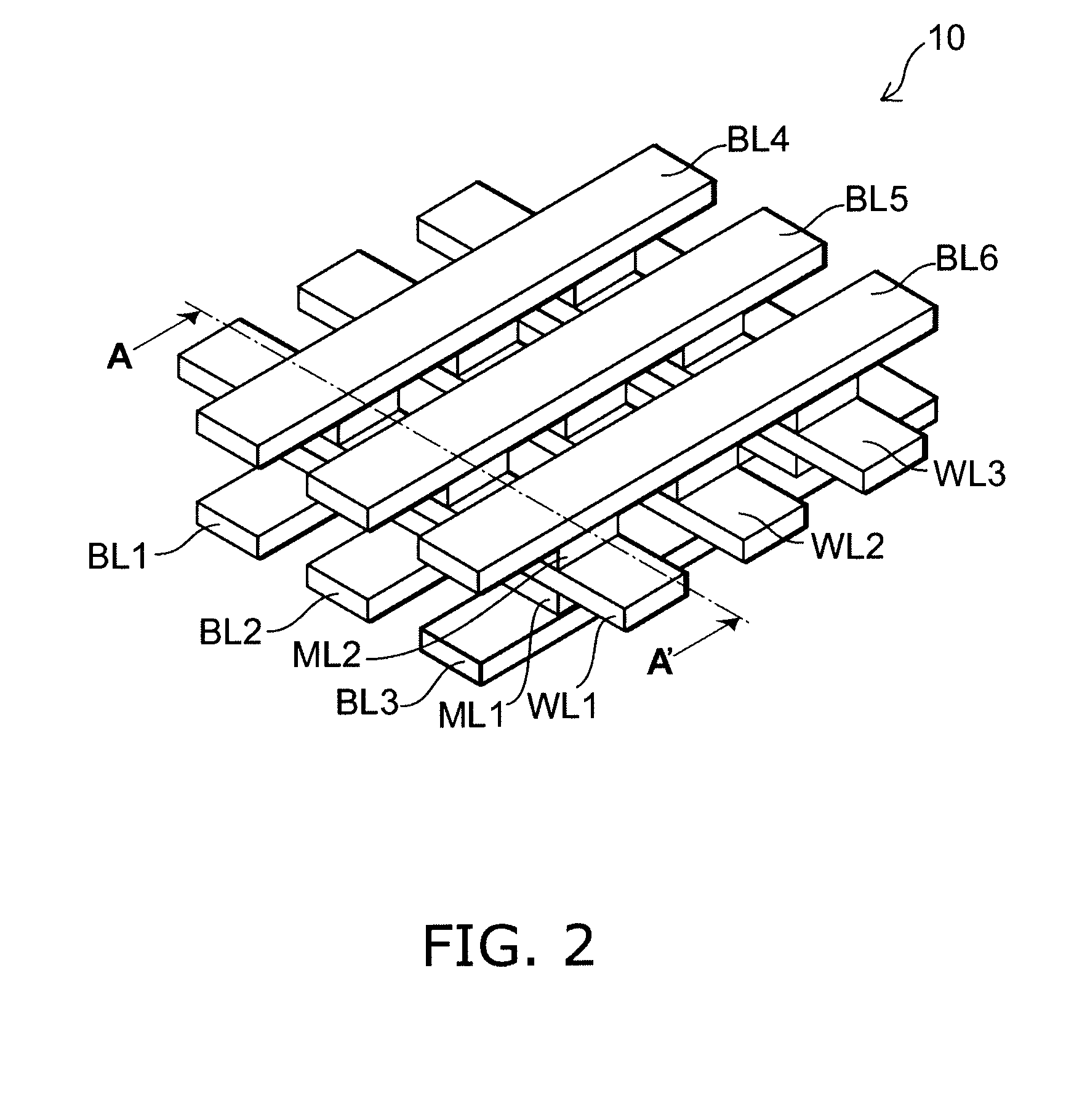
[0031]FIG. 2 is a schematic perspective view illustrating the structure of the nonvolatile storage device according to the first embodiment of the present invention.
[0032]As illustrated in FIG. 1 and FIG. 2, a nonvolatile storage device 10 according to the first embodiment of the present invention includes a resistance change memory having two laminated crosspoint cell layers. Each nonvolatile memory element includes a plurality of unit cells C11, C12, C13, C14, C15, C16, C21, C22, C23, C24, C25, C26, C31, C32, C33, C34, C35, and C36 arranged in a matrix configuration. Each unit cell is defined by a plurality of bit lines BL1, BL2, BL3, BL4, BL5, and BL6, and by a plurality of word lines WL1, WL2, and WL3. At each crosspoint, where a word line and a bit line intersect three dimensionally, for example, a variable resistance ...
first example
[0066]A first example according to this embodiment will now be described.
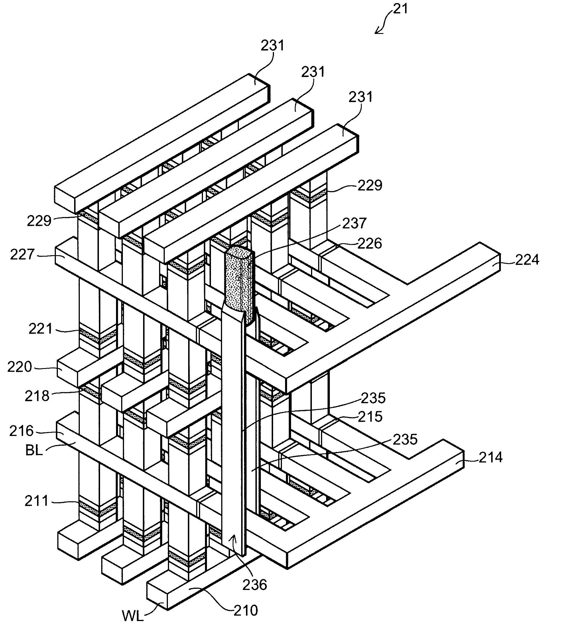
[0067]A nonvolatile storage device 11 according to the first example is an example in which SGT transistors that collectively select bit lines in a plane parallel to a major surface of a substrate is used as the layer selection transistors. The SGT transistor is a vertical transistor including a channel along a direction perpendicular to the major surface of the substrate. A gate electrode is provided opposite to a face of the channel that lies along a direction perpendicular to the major surface of the substrate and is provided to surround the channel. In this structure, the gate electrode of the SGT transistor essentially surrounds the channel completely. Hence, the dominance of the gate is strong, and the cut-off characteristics are excellent. This structure is therefore suitable as the layer selection transistor. Additionally, in the case where an SGT transistor is used, the layer selection transistors can ...
second embodiment
[0103]FIG. 9 is a circuit configuration diagram illustrating a structure of a nonvolatile storage device according to a second embodiment of the present invention.
[0104]As illustrated in FIG. 9, a nonvolatile storage device 20 according to the second embodiment of the present invention uses layer selection transistors that select a series of bit lines laminated in two layers.
[0105]Namely, layer selection transistors TR1, TR2, and TR3 are provided to select the recording layers of the first layer; layer selection transistors TR4, TR5, and TR6 are provided to select the recording layers of the second layer; and the laminated recording layers are selected by the layer selection transistors TR1 to TR6.
[0106]The gate electrodes of the layer selection transistor TR1 that selects the first memory layer and the layer selection transistor TR4 that selects the second memory layer have a common potential. Likewise, the gate electrodes of the layer selection transistors TR2 and TR5 have a commo...
PUM
 Abstract
Description
Claims
Application Information