Thin film transistor
a thin film transistor and carbon nanotube technology, applied in the field of thin film transistors, can solve the problems of low carrier mobility, high cost, complicated method of making p-si tft,
- Summary
- Abstract
- Description
- Claims
- Application Information
AI Technical Summary
Benefits of technology
Problems solved by technology
Method used
Image
Examples
first embodiment
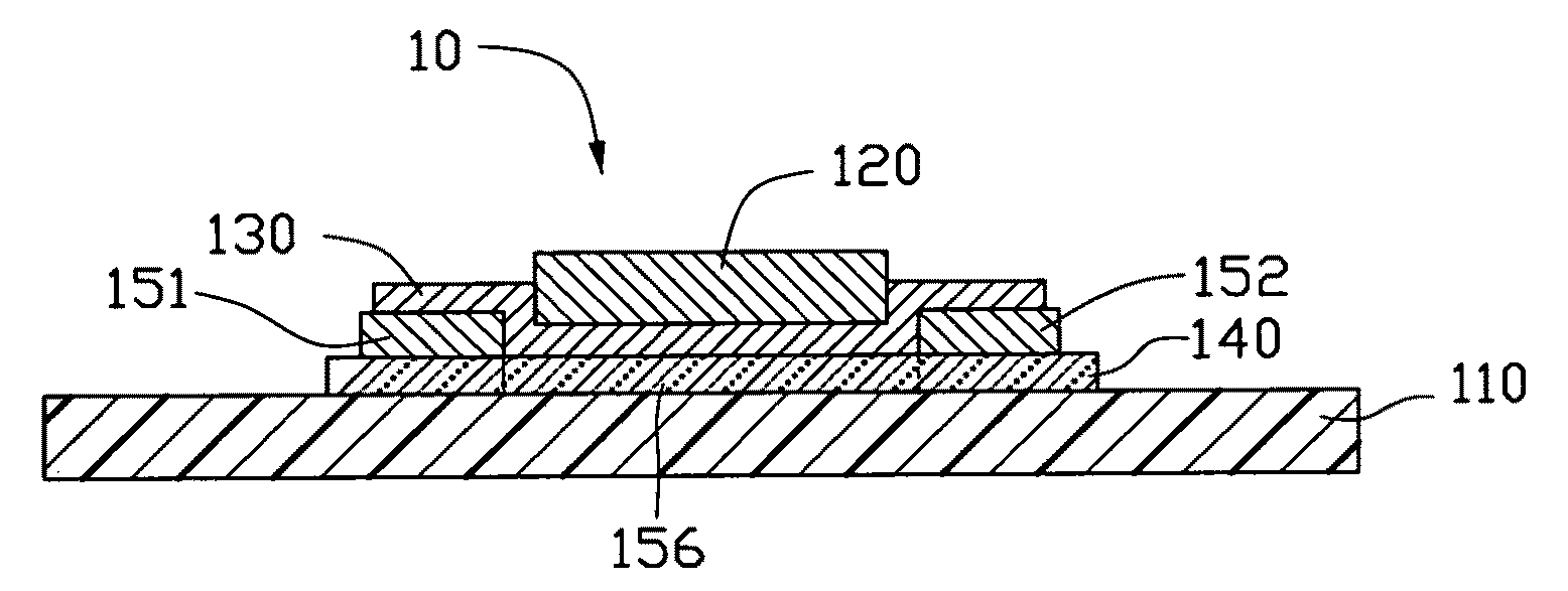
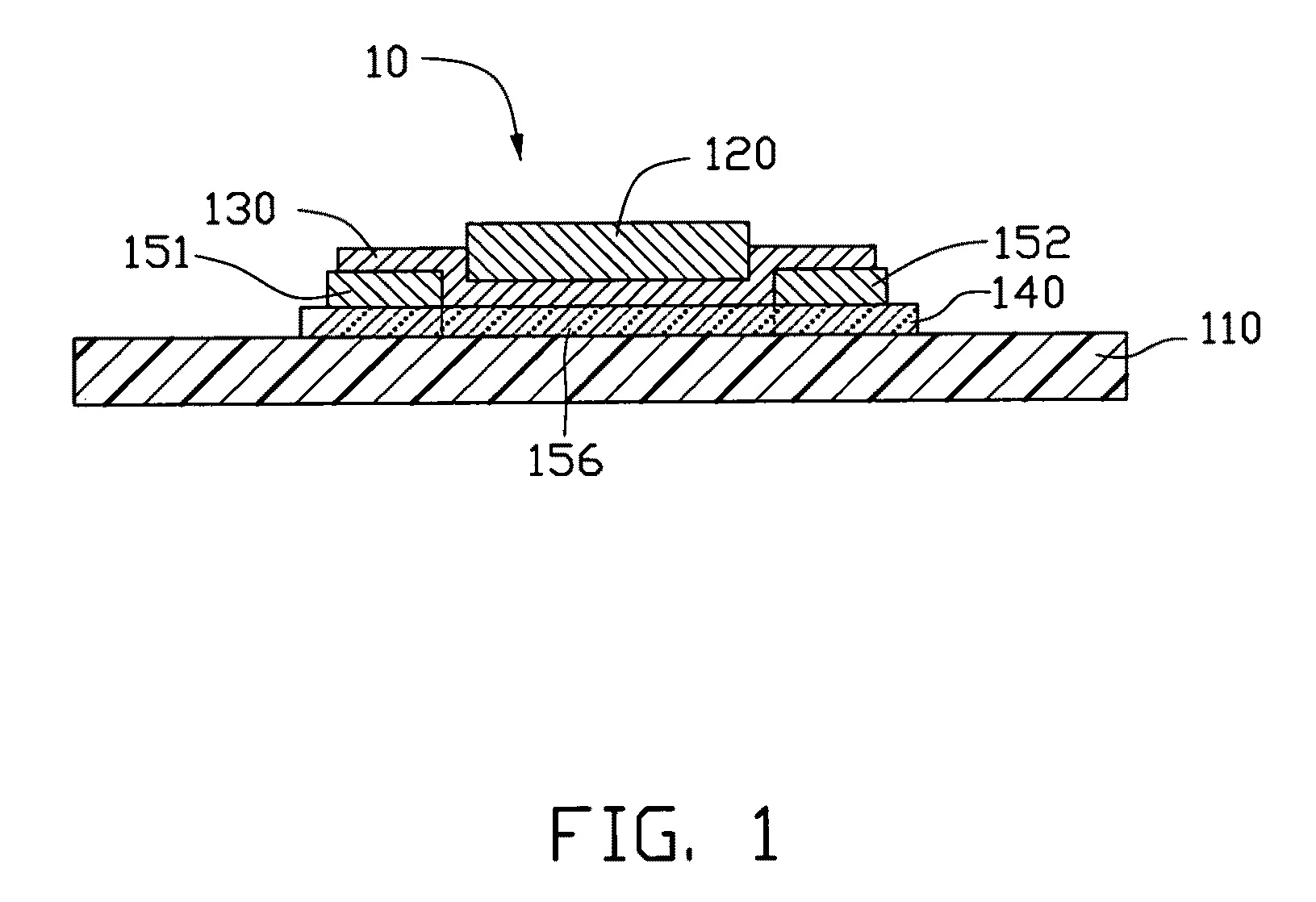
[0020]Referring to FIG. 1, a thin film transistor 10 is provided in a first embodiment, and has a top gate structure. The thin film transistor 10 includes a semiconducting layer 140, a source electrode 151, a drain electrode 152, an insulating layer 130, and a gate electrode 120. The thin film transistor 10 is disposed on an insulating substrate 110.
[0021]The semiconducting layer 140 is disposed on the insulating substrate 110. The source electrode 151 and the drain electrode 152 are spaced therebetween and electrically connected to the semiconducting layer 140. The insulating layer 130 is disposed between the semiconducting layer 140 and the gate electrode 120. The insulating layer 130 is disposed at least on the semiconducting layer 140, or covers the semiconducting layer 140, the source electrode 151, and the drain electrode 152. The gate electrode 120 is disposed on the insulating layer 130. The gate electrode 120 is disposed above the semiconducting layer 140 and insulating fro...
second embodiment
[0033]Referring to FIG. 5, a thin film transistor 20 is provided in a second embodiment and has a bottom gate structure. The thin film transistor 20 includes a gate electrode 220, an insulating layer 230, a semiconducting layer 240, a source electrode 251, and a drain electrode 252. The thin film transistor 20 is disposed on an insulating substrate 210.
[0034]The structure of the thin film transistor 20 in the second embodiment is similar to the thin film transistor 10 in the first embodiment. The difference is that, in the second embodiment, the gate electrode 220 is disposed on the insulating substrate 210. The insulating layer 230 covers the gate electrode 220. The semiconducting layer 240 is disposed on the insulating layer 230, and insulated from the gate electrode 220 by the insulating layer 230. The source electrode 251 and the drain electrode 252 are spaced apart from each other and electrically connected to the semiconducting layer 240. The source electrode 251, and the drai...
PUM
| Property | Measurement | Unit |
|---|---|---|
| thickness | aaaaa | aaaaa |
| diameter | aaaaa | aaaaa |
| thickness | aaaaa | aaaaa |
Abstract
Description
Claims
Application Information
 - R&D Engineer
- R&D Manager
- IP Professional
- Industry Leading Data Capabilities
- Powerful AI technology
- Patent DNA Extraction
Browse by: Latest US Patents, China's latest patents, Technical Efficacy Thesaurus, Application Domain, Technology Topic, Popular Technical Reports.
© 2024 PatSnap. All rights reserved.Legal|Privacy policy|Modern Slavery Act Transparency Statement|Sitemap|About US| Contact US: help@patsnap.com


