Plasma process with photoresist mask pretreatment

a technology of photoresist mask and pretreatment, which is applied in the direction of decorative surface effects, electrical appliances, decorative arts, etc., can solve the problems easy and undetectable etching or damage of thin and weak photoresist mask, and the lik

Inactive Publication Date: 2009-11-19
LAM RES CORP
View PDF13 Cites 597 Cited by
  • Summary
  • Abstract
  • Description
  • Claims
  • Application Information

AI Technical Summary

Benefits of technology

[0005]To achieve the foregoing and in accordance with the purpose of the present invention, a method for etching features in a dielectric layer through a photoresist (PR) mask is provided. The PR mask is patterned using laser light having a wavelength not more than 193 nm. The PR mask is pre-treated with a noble gas plasma, and then a plurality of cycles of a plasma process is provided. Each cycle includes a deposition phase that deposits a deposition layer over the PR mask, the deposition layer covering a top and sidewalls of mask features of the PR mask, and a shaping phase that shapes the deposition layer deposited over the PR mask.

Problems solved by technology

Such small circuit features require higher resolution and thus a thinner photoresist because of the depth-of-focus (depth-of-field) limitations of the patterning image.
The photoresist material is also softer and weaker, and such a thin and weak photoresist mask would easily and undesirably be etched or damaged during a plasma process after the patterned photoresist mask is provided.

Method used


Image

  • Plasma process with photoresist mask pretreatment
  • Plasma process with photoresist mask pretreatment
  • Plasma process with photoresist mask pretreatment

Examples


Embodiment Construction

[0019]The present invention will now be described in detail with reference to a few preferred embodiments thereof as illustrated in the accompanying drawings. In the following description, numerous specific details are set forth in order to provide a thorough understanding of the present invention. It will be apparent, however, to one skilled in the art, that the present invention may be practiced without some or all of these specific details. In other instances, well known process steps and / or structures have not been described in detail in order to not unnecessarily obscure the present invention.

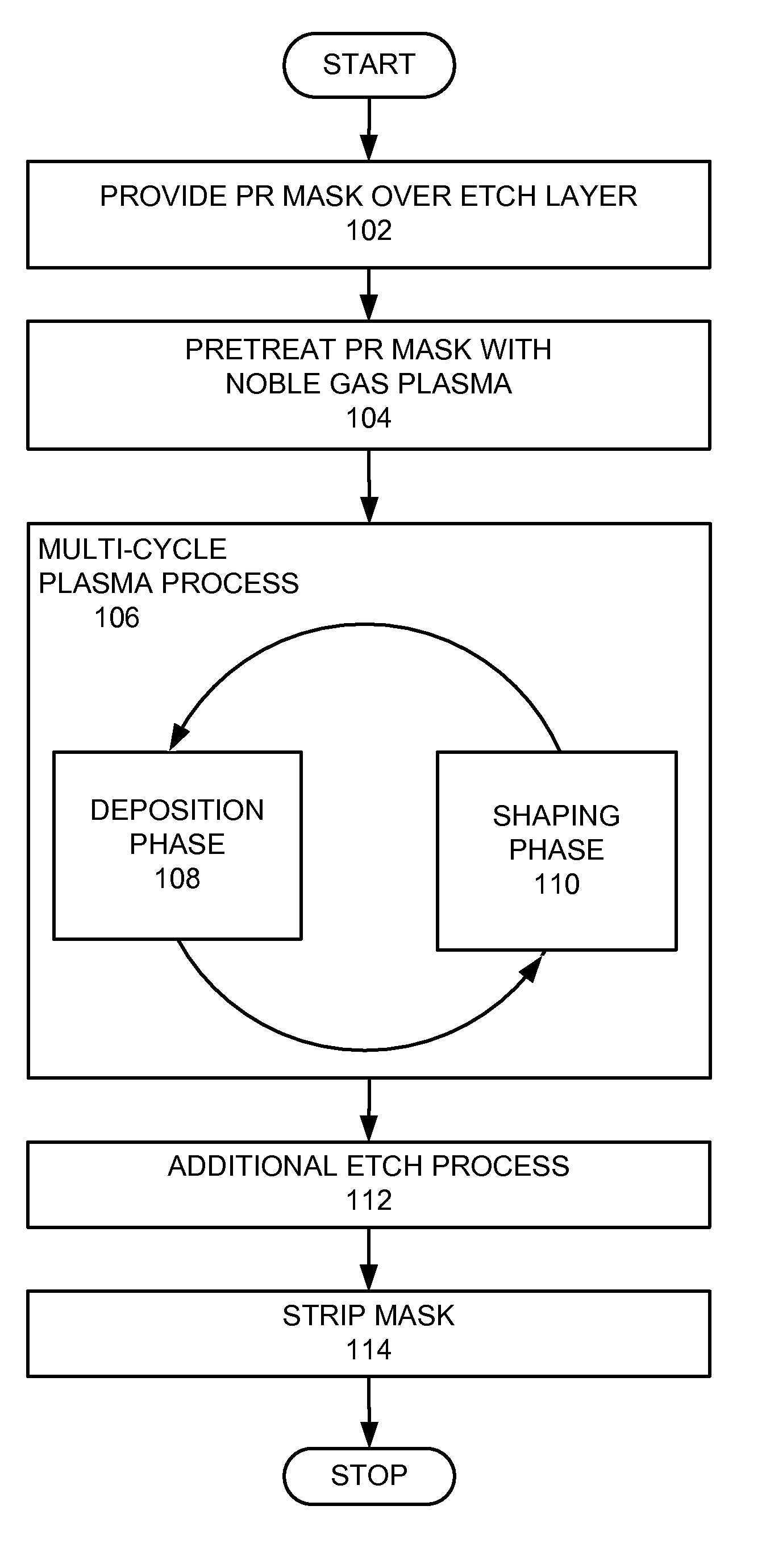
[0020]To facilitate understanding, FIG. 1 is a high level flow chart of a plasma process with a PR mask pretreatment in accordance with one embodiment of the present invention. A patterned photoresist (PR) mask is provided over an etch layer (step 102).

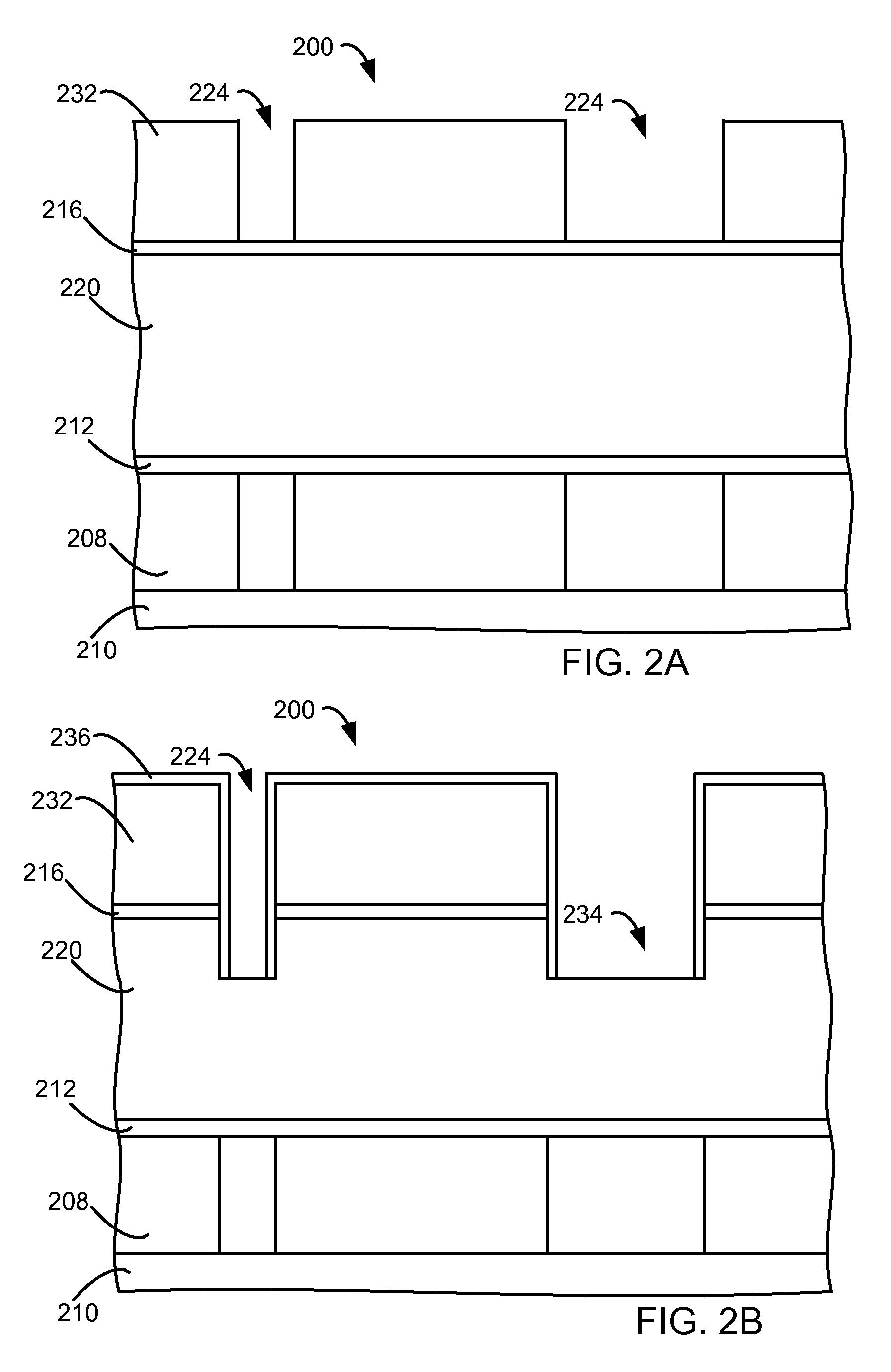
[0021]FIG. 2A is a cross-sectional view of an example of a stack 200 processed in accordance with one embodiment of the present invention. ...


PUM

PropertyMeasurementUnit
wavelengthaaaaaaaaaa
frequencyaaaaaaaaaa
frequencyaaaaaaaaaa

Abstract

A method for etching features in a dielectric layer through a photoresist (PR) mask is provided. The PR mask is patterned using laser light having a wavelength not more than 193 nm. The PR mask is pre-treated with a noble gas plasma, and then a plurality of cycles of a plasma process is provided. Each cycle includes a deposition phase that deposits a deposition layer over the PR mask, the deposition layer covering a top and sidewalls of mask features of the PR mask, and a shaping phase that shapes the deposition layer deposited over the PR mask.

Description

BACKGROUND OF THE INVENTION[0001]The invention relates to the formation of semiconductor devices. More specifically, the invention relates to the formation of semiconductor devices by etching features in an etch layer through a photoresist (PR) mask.[0002]During semiconductor wafer processing, features of the semiconductor device are defined in the wafer using well-known patterning and etching processes. In these processes, a photoresist (PR) material is deposited on the wafer and then is exposed to light filtered by a reticle. The reticle may be a glass plate that is patterned with exemplary feature geometries that block light from propagating through the reticle.[0003]After passing through the reticle, the light contacts the surface of the photoresist material. The light changes the chemical composition of the photoresist material such that a developer can remove a portion of the photoresist material. In the case of positive photoresist materials, the exposed regions are removed, ...

Claims


Application Information

Patent Timeline
Patent Type & Authority Applications(United States)
IPC IPC(8): H01L21/3205
CPCH01L21/0273H01L21/31138H01L21/76816H01L21/76802H01L21/31144
Inventor HEO, DONGHOKIM, JI SOO
Owner LAM RES CORP
Why Eureka
Try Eureka