Electrode and Vacuum Processing Apparatus
a vacuum processing and electrode technology, applied in the direction of chemical vapor deposition coating, coating, plasma technique, etc., can solve the problems of difficult to improve the film quality, degrade the film quality, and non-uniform distribution of the film deposited on the substrate, so as to improve the speed of film deposition on the substrate to be processed, improve the uniform distribution of the deposited film, and improve the effect of film deposition speed
- Summary
- Abstract
- Description
- Claims
- Application Information
AI Technical Summary
Benefits of technology
Problems solved by technology
Method used
Image
Examples
first embodiment
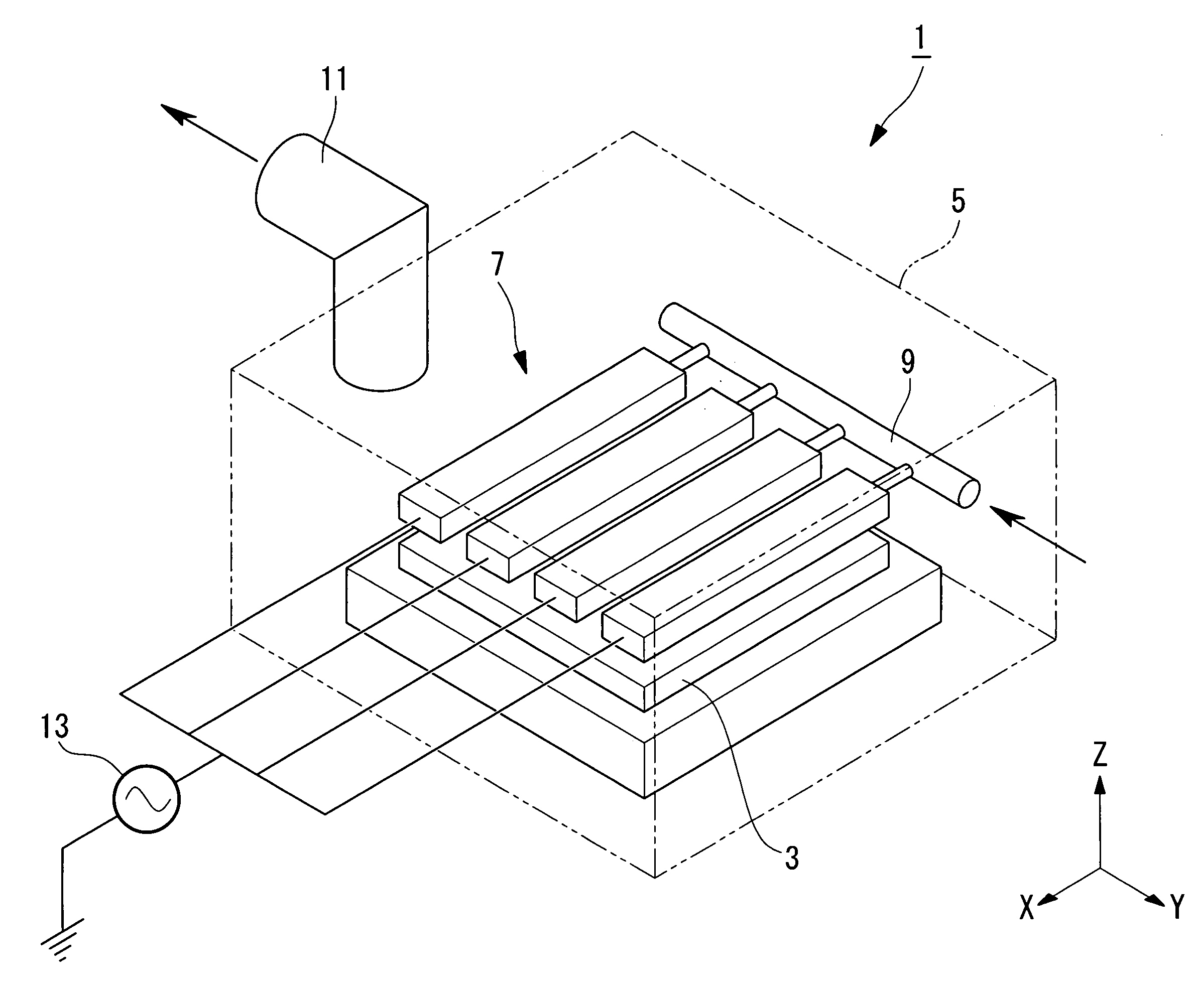
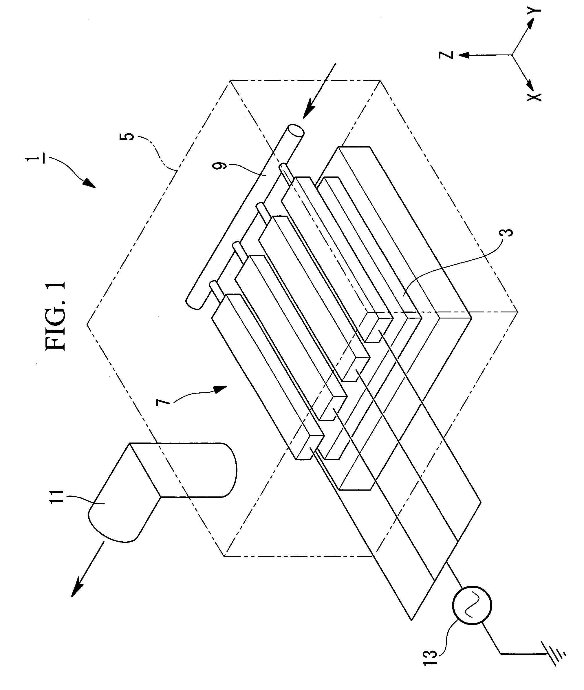
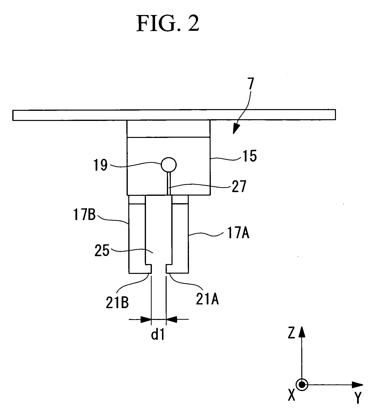
[0055]Hereinafter, a plasma CVD apparatus according to a first embodiment of the present invention will be described with reference to FIGS. 1 to 3.
[0056]FIG. 1 is a schematic view for explaining the structure of the plasma CVD apparatus according to the present embodiment.
[0057]As shown in FIG. 1, the plasma CVD apparatus (vacuum processing apparatus) 1 has: a chamber (casing) 5 that accommodates a substrate (substrate to be processed) 3 on which a film is deposited; electrode units 7 that perform plasma discharge toward the substrate 3; a supplier 9 that supplies a reactant gas; an exhauster 11 that exhausts the reactant gas; and a power feeder 13 that supplies high-frequency power to the electrode units 7.
[0058]The chamber 5 includes: the supplier 9 that supplies the reactant gas to the inside; the exhauster 11 that exhausts the reactant gas which has been used for film deposition; the power feeder 13 that supplies the high-frequency power used for plasma formation; and a pump (n...
second embodiment
[0085]Next, a second embodiment of the present invention will be described with reference to FIG. 4.
[0086]Although the basic structure of a plasma CVD apparatus of the present embodiment is similar to that of the first embodiment, the structure of the electrode units of the present embodiment is different from that of the first embodiment. Therefore, in the present embodiment, only the surroundings of the electrode units will be described by using FIG. 4, and description of the other elements and the like is omitted.
[0087]FIG. 4 is a partial cross-sectional view for explaining the structure of the electrode units and the flow of the reactant gas in the plasma CVD apparatus according to the present embodiment.
[0088]The same elements as those of the first embodiment are denoted by the same reference numerals and description thereof is omitted.
[0089]As shown in FIG. 4, electrode units 107 of the plasma CVD apparatus (vacuum processing apparatus) 101 each have a mount 115 and the electr...
third embodiment
[0099]Next, a third embodiment of the present invention will be described with reference to FIG. 5.
[0100]Although the basic structure of a plasma CVD apparatus of the present embodiment is similar to that of the first embodiment, the structure of the electrode units thereof is different from that of the first embodiment. Therefore, in the present embodiment, only the surroundings of the electrode units will be described by using FIG. 5, and description of the other elements and the like is omitted.
[0101]FIG. 5 is a partial cross-sectional view for explaining the structure of the electrode units and the flow of the reactant gas in the plasma CVD apparatus according to the present embodiment.
[0102]The same elements as those of the first embodiment are denoted by the same reference numerals and description thereof is omitted.
[0103]As shown in FIG. 5, electrode units 207 of the plasma CVD apparatus (vacuum processing apparatus) 201 each have a mount 215 and electrodes 217A and 217B.
[010...
PUM
| Property | Measurement | Unit |
|---|---|---|
| Peclet number | aaaaa | aaaaa |
| diameter | aaaaa | aaaaa |
| diameter | aaaaa | aaaaa |
Abstract
Description
Claims
Application Information


