

Connection/separation element in photoelectric converter portion, solid-state imaging device, and imaging apparatus
a technology of separation element and photoelectric converter, which is applied in the direction of television system scanning details, radioation control devices, television systems, etc., can solve the problems of increasing apparatus size and increasing cost, and achieve the effect of suppressing sensitivity deterioration
- Summary
- Abstract
- Description
- Claims
- Application Information
AI Technical Summary
Benefits of technology
Problems solved by technology
Method used
Image

Examples
first embodiment
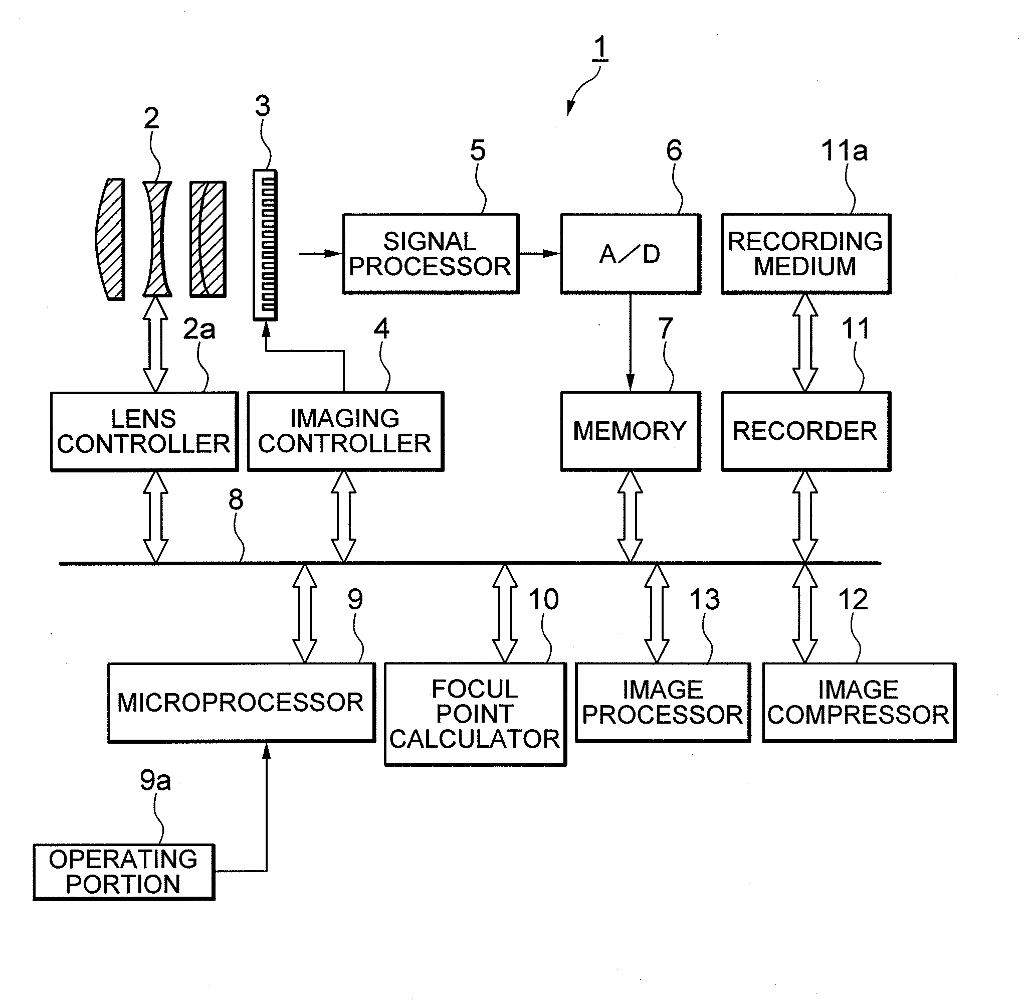
[0052]FIG. 1 is a block diagram showing an electronic camera 1 as an imaging apparatus according to a first embodiment of the present invention. The electronic camera 1 is equipped with an image-taking lens 2. The image-taking lens 2 is controlled by a lens controller 2a upon focusing and stopping down of an aperture stop. An imaging surface of a solid-state imaging device 3 for performing photoelectric conversion of an object image formed by the image-taking lens 2 is disposed in the image side space of the image-taking lens 2.
[0053]The solid-state imaging device 3 is driven by an instruction of an imaging controller 4 and outputs a signal. The signal output from the solid-state imaging device 3 is either an imaging signal for forming an image signal showing the object image or a focal point detection signal for detecting focal point adjusting state of the image-taking lens 2. Either way a signal is processed by a signal processor 5 and an A / D converter 6, and stored temporarily in...
second embodiment
[0140]FIG. 17 is a plan view showing an imaging area 31, in particular, of a solid-state imaging device 103 of an electronic camera according to a second embodiment of the present invention corresponding to FIG. 3.
[0141]FIG. 18 is an enlarged view enlarged any area of an imaging area 31 shown in FIG. 17 corresponding to FIG. 4. FIG. 19 is a flow chart schematically showing movement of the electronic camera according to the second embodiment of the present invention. In FIG. 17 or 18, the same or similar component as in FIG. 3 or 4 is attached the same symbol to eliminate duplicated explanations.
[0142]The point where the present embodiment is different from the first embodiment is that any specific area such as the focal point detection areas 32 through 37 are not disposed in the imaging area 31, all pixels 20 of effective area are the pixel 20V shown in FIGS. 6 through 11, and the electronic camera 1 according to the present embodiment carries out the movement shown in FIG. 19.
[0143...
third embodiment
[0153]FIG. 20 is a plan view showing an imaging area 31, in particular, of a solid-state imaging device 203 of an electronic camera according to a third embodiment of the present invention corresponding to FIGS. 3 and 17. FIG. 21 is an enlarged view enlarged any area of an imaging area 36 shown in FIG. 20 corresponding to FIGS. 4 and 18. In FIGS. 20 and 21, the same or similar component as in FIG. 3, 4, 17 or 18 is attached the same symbol to eliminate duplicated explanations.
[0154]The point where the present embodiment is different from the first embodiment is that pixels 20 of only the focal point detection areas 32, 36, 37 extending in X direction are pixels 20H shown in FIG. 12, and the rest of pixels 20 are pixels 20V shown in FIGS. 6 through 11.
[0155]With the present embodiment, the focal point adjusting state can be detected on the basis of the signal of each pixel of the pixel column in Y-axis direction corresponding to the position of the object similar to the second embodi...
PUM
 Abstract
Description
Claims
Application Information