Supercharge Your Innovation With Domain-Expert AI Agents!

Liquid crystal display panel

a technology of liquid crystal display and display panel, which is applied in the direction of instruments, static indicating devices, etc., can solve the problem of raising the cost of the lcd panel b>1/b>

Inactive Publication Date: 2009-12-03
INNOLUX CORP +1
View PDF4 Cites 10 Cited by
  • Summary
  • Abstract
  • Description
  • Claims
  • Application Information

AI Technical Summary

Benefits of technology

The present patent relates to an LCD panel that includes a p-type transistor and an n-type transistor in each pixel, which helps to decrease the cost of manufacturing the panel and increase the aperture ratio. The panel includes m scanning lines, data lines, and pixel pairs. The scanning drivers and data drivers provide the necessary signals to turn on or off the transistors in the pixels. The waveform of the scanning signals is designed to ensure that each pixel is turned on for a short time period, reducing power consumption. The technical effect of this design is to improve the performance and cost-effectiveness of LCD panels.

Problems solved by technology

As the size of the LCD panel 1 increases, the number of required data drivers 15 increases, raising the cost of the LCD panel 1.

Method used


Image

  • Liquid crystal display panel
  • Liquid crystal display panel
  • Liquid crystal display panel

Examples


first embodiment

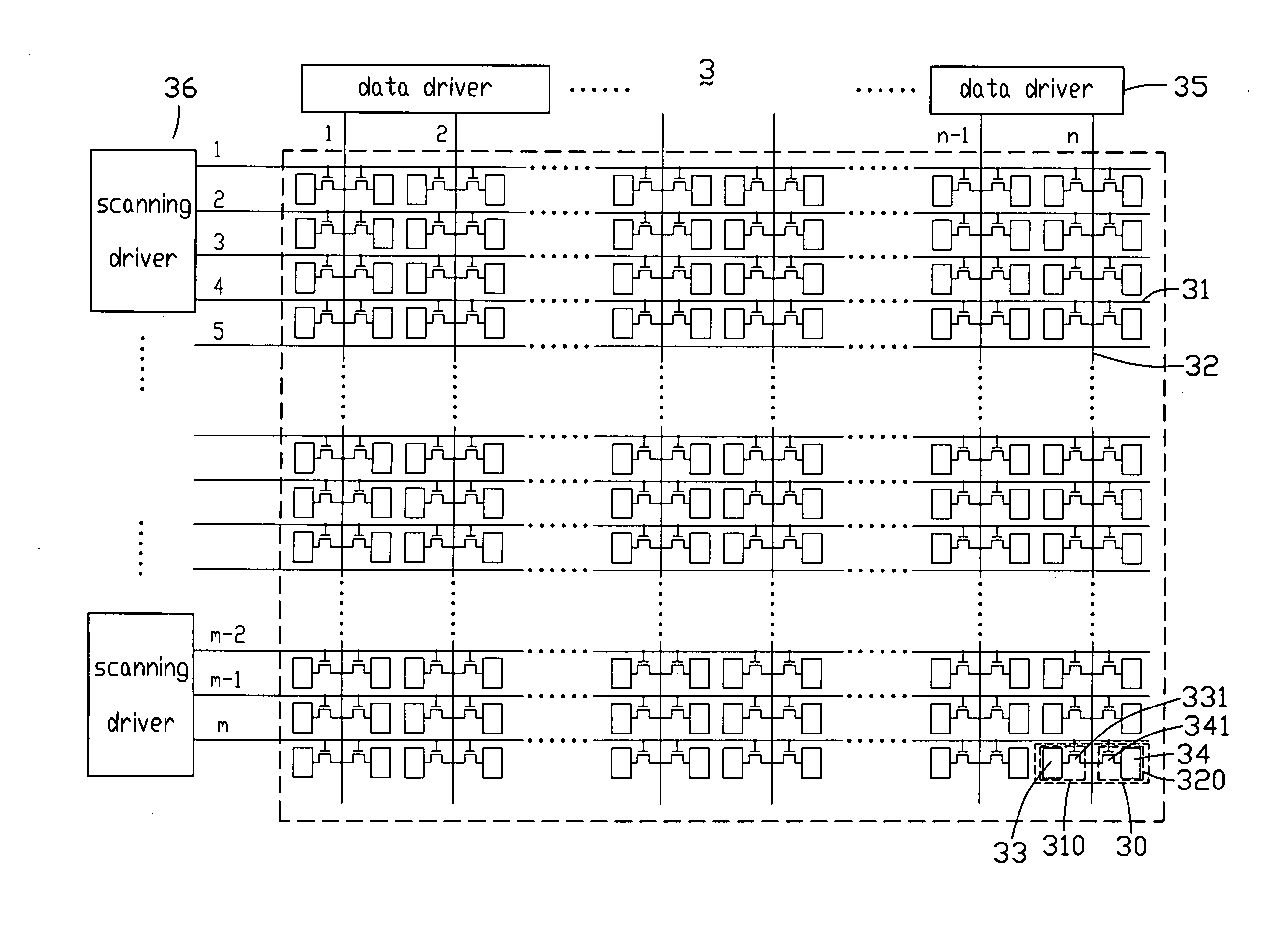
[0014]FIG. 1 is a circuit diagram of an LCD panel according to the present disclosure. The LCD panel 3 includes m scanning lines 31, n data lines 32, a plurality of pixel pairs 30, a plurality of scanning drivers 36, and a plurality of data drivers 35. The scanning drivers 36 and the data drivers 35 drive the scanning lines 31 and the data lines 32, respectively.

[0015]Each pixel pair 30 includes a first pixel 310 and a second pixel 320. Each first pixel 310 includes a first pixel electrode 33 and a first TFT 331. Each second pixel 320 includes a second pixel electrode 34 and a second TFT 341. Gate electrodes of the first TFT 331 and the second TFT 341 of each pixel pair 30 are connected to a single scanning line 31. Source electrodes of the first TFT 331 and the second TFT 341 of each pixel pair 30 are connected to a single data line 32. Drain electrodes of the first TFT 331 and the second TFT 341 of each pixel pair 30 are connected to the first pixel electrode 33 and the second pix...

second embodiment

[0020]FIG. 3 shows an LCD panel according to the present disclosure, differing from LCD panel 3 only in that each pixel pair 40 includes a first pixel 410 and a second pixel 420. The first pixel 410 and the second pixel 420 are arranged on two sides of a corresponding scanning line 41, and are arranged on one side of a corresponding data line 42. The first pixel 410 and the second pixel 420 are connected to a single scanning line 41, and are connected to a single data line 42. Each pixel pair 40 is arranged every two scanning lines 31 in each column along the data lines 42. That is, the pixel pairs 40 are arranged alternatively on two sides of the data lines 42. The LCD panel 4 has advantages similar to those of the LCD panel 3.

third embodiment

[0021]FIG. 4 shows an LCD panel according to the present disclosure, differing from LCD panel 3 only in that each pixel pair 50 includes a first pixel 510 and a second pixel 520. The first pixel 510 and the second pixel 520 are connected to a single data line 42, and are connected to two adjacent scanning lines 41 respectively. That is, the first pixel 510 and the second pixel 520 are arranged alternatively on two sides of a corresponding data line 52. The LCD panel 5 has advantages similar to those of the LCD panel 3.


PUM


Abstract

A liquid crystal display (LCD) panel includes scanning lines to receive scanning signals, data lines to receive data signals; and pixel pairs. Each pixel pair includes a first pixel and a second pixel. The first pixel includes a first thin film transistor (TFT), and the second pixel includes a second TFT. The first pixel and the second pixel of each pixel pair are arranged on two sides of the data line in each row, and connected to a single data line via the first TFT and the second TFT respectively. One of the two TFTs is a p-type TFT, and the other one is an n-type TFT.

Description

BACKGROUND[0001]1. Technical Field[0002]The present disclosure relates to liquid crystal displays (LCD), and particularly to an LCD panel having a p-type transistor and an n-type transistor in one pixel.[0003]2. Description of Related Art[0004]Because LCD panels have advantages of portability, low power consumption, and low radiation, they have been widely used in various portable information products such as notebooks, personal digital assistants (PDAs), video cameras, and the like.[0005]Referring to FIG. 5, a commonly used LCD panel 1 includes a plurality of scanning lines 11, a plurality of data lines 12, a plurality of pixels 13, a plurality of thin film transistors (TFTs) 14, a scanning driver 16, and a data driver 15.[0006]The data driver 15 provides data signals to the pixels 13 via the data lines 12 when the TFTs 14 are turned on. The scanning driver 16 provides scanning voltages to the scanning lines 11 to switch the TFTs 13 on or off. Each output terminal (not shown) of th...

Claims


Application Information

Patent Timeline
Patent Type & Authority Applications(United States)
IPC IPC(8): G09G3/36
CPCG09G3/3607G09G2300/0426G09G3/3648
Inventor SU, XIN
Owner INNOLUX CORP
Features
  • R&D
  • Intellectual Property
  • Life Sciences
  • Materials
  • Tech Scout
  • Unparalleled Data Quality
  • Higher Quality Content
  • 60% Fewer Hallucinations
Learn More