

Plasma display device
- Summary
- Abstract
- Description
- Claims
- Application Information
AI Technical Summary
Benefits of technology
Problems solved by technology
Method used
Image

Examples
first embodiment
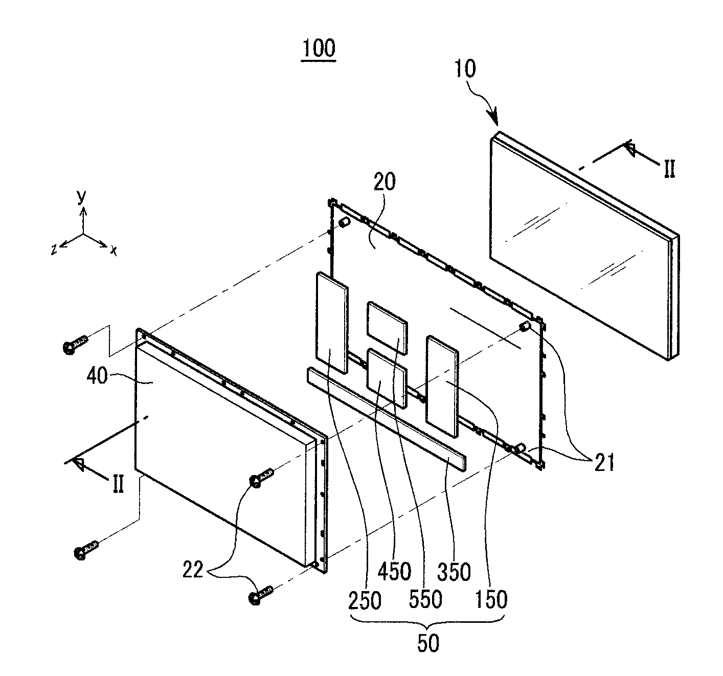
[0026]FIG. 1 is an exploded perspective view of a plasma display device 100 according to the present invention.
[0027]Referring to FIG. 1, the plasma display device 100 includes a plasma display panel (PDP) 10 for displaying an image, a chassis base 20, a heat dissipating plate 40, and a plurality of printed circuit boards 50.
[0028]The chassis base 20 supports the PDP and is attached to an opposite side of the PDP 10 from the display side of the PDP 10. The heat dissipating plate 40 is disposed at and attached to the rear of the chassis base 20. As such, the chassis base 20 includes a plurality of bosses 21 separated from each other for receiving the heat dissipating plate 40. The heat dissipating plate 40 may be fastened to the bosses 21 by screws 22 or by other suitable fasteners.
[0029]The printed circuit boards 50 are disposed between the chassis base 20 and the heat dissipating plate 40 and attached to the heat dissipating plate 40. Also, the printed circuit boards 50 may be elec...
second embodiment
[0050]FIG. 3 is a cross-sectional view of a plasma display device 200 according to the present invention, and FIG. 4 is a partial exploded perspective view of a printed circuit board, a switch, and a heat sink shown in FIG. 3.
[0051]Referring to FIGS. 3 and 4, the plasma display device 200 according to the second embodiment further includes a heat sink 72.
[0052]A switch 60 is installed on the inner surface of a heat dissipating plate 40 through an installation hole 41 and a screw 19. The heat sink 72 is installed on the outer surface of the heat dissipating plate 40, corresponding to the switch 60.
[0053]The heat sink 72 may protrude in the z-axis direction within a suitable range of space between the heat dissipating plate 40 and a back cover (not shown). Specifically, the heat sink 72 may be provided on the outer surface of the heat dissipating plate 40 within a range such that it protrudes without increasing the overall thickness (z-axis direction) of the plasma display device 200....
third embodiment
[0056]FIG. 5 is a cross-sectional view of a plasma display device 300 according to the present invention.
[0057]Referring to FIG. 5, the plasma display device 300 according to the third embodiment includes a switch 60 and a heat sink 372 in different locations from previously described embodiments.
[0058]The heat dissipating plate 40 includes a plane portion 42, a side portion 43, and a flange 44 forming a 3-dimensional space for accommodating printed circuit boards 50, for example, a scan board 250.
[0059]The plane portion 42 is formed at the rear of the scan board 250 and is generally parallel to the scan board 250 and a chassis base 20. Specifically, the plane portion 42 defines the rearmost part of the heat dissipating plate 40.
[0060]The side portion 43 is curved from the plane portion 42 toward the chassis base 20. Specifically, the side portion 43 defines the side of the heat dissipating plate 40 and is generally perpendicular to the plane portion 42.
[0061]The flange 44 is curved...
PUM
 Abstract
Description
Claims
Application Information