Method for bonding wafers

a technology of bonding wafers and methods, applied in the direction of measuring devices, instruments, electrical equipment, etc., can solve the problems of slipping relative to one another, risk of wafers which have previously been positioned exactly,

Active Publication Date: 2009-12-03
THALLNER ERICH
View PDF12 Cites 0 Cited by
  • Summary
  • Abstract
  • Description
  • Claims
  • Application Information

AI Technical Summary

Benefits of technology

[0009]It is the object of the invention to provide a method and a device with which disk-shaped parts, especially semiconductor disks, can be exactly aligned and joined together in the best possible fashion.
[0024]In this way a device which manages without contact pins is created from which it follows that no gaps are formed on the contact surfaces of the corresponding surfaces of the wafers. Furthermore, the device according to the invention has the advantage that a precise alignment only takes place after the corresponding surfaces of the wafers have been brought in contact. As a result, any slippage of the wafers after alignment by the alignment means can be eliminated. A substantially more accurate alignment of the two wafers is achieved whereby the quality of the wafers produced using the device according to the invention increases significantly.

Problems solved by technology

Firstly, gaps are formed by the spacers in the contact surface and on the other hand, during contacting by withdrawing the spacers there is the risk that the wafers which have previously been positioned exactly, slip relative to one another.

Method used


Image

  • Method for bonding wafers
  • Method for bonding wafers

Examples


Embodiment Construction

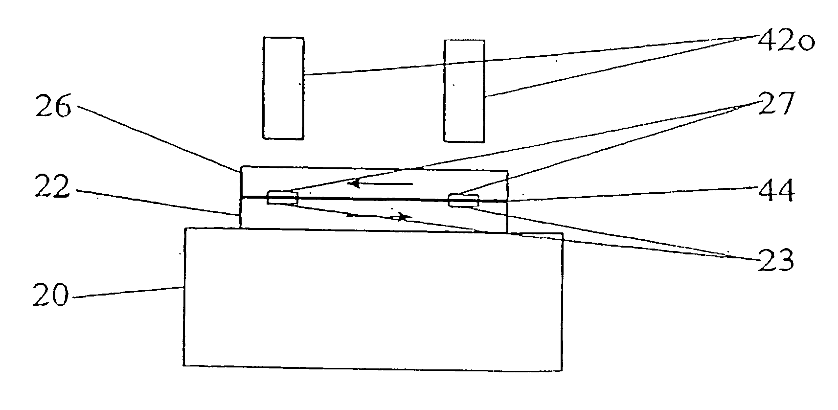
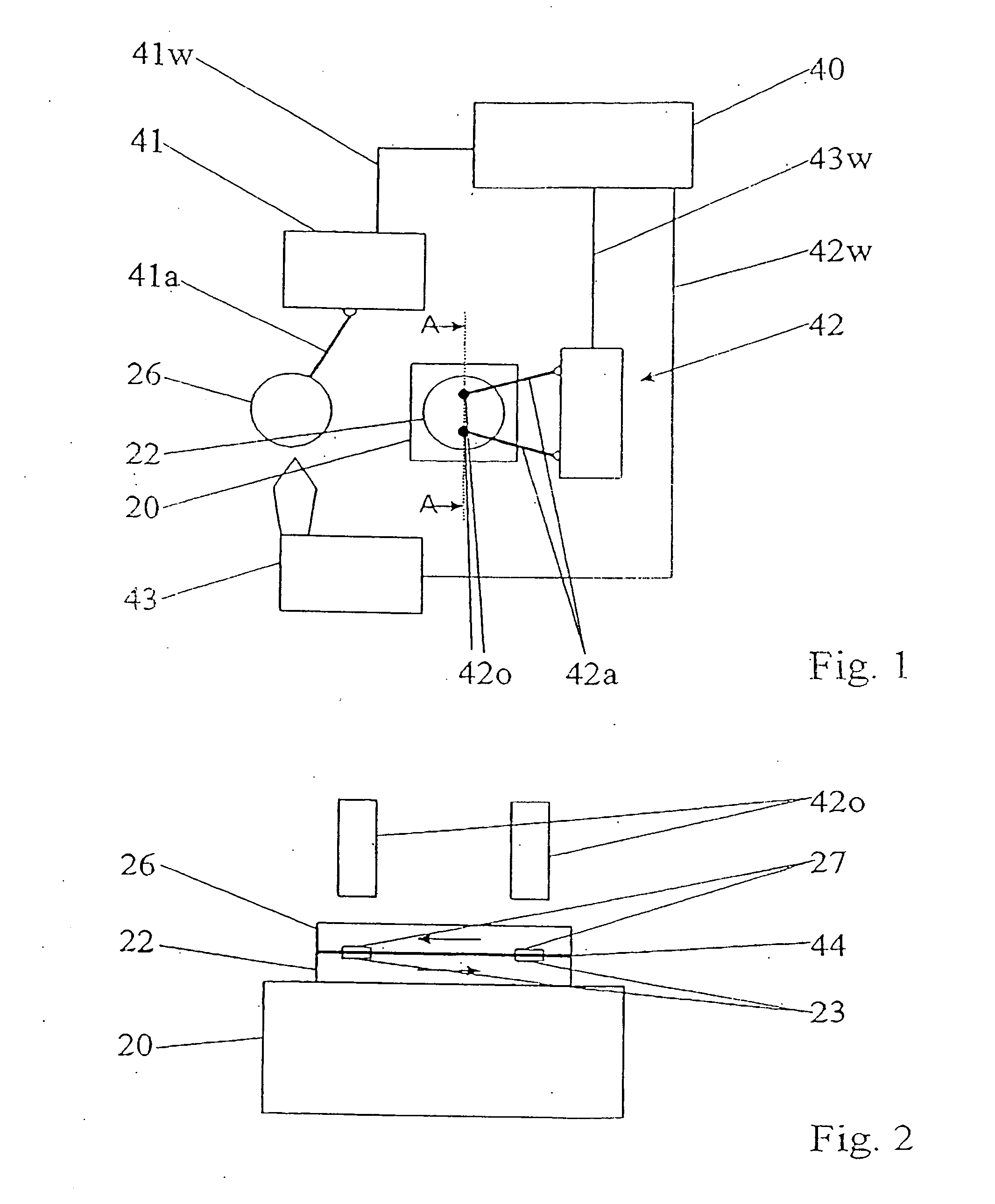
[0043]FIG. 1 is a highly schematic diagram showing a control unit 40 which executes the method according to the process steps described in the above description in an exemplary embodiment of the present invention.

[0044]The control unit 40 here is connected in each case by a first, second and third operative connection 41w, 42w and 43w to a device 41 for receiving and aligning the second wafer 26, to a detection device 42 to detect the position of the wafers relative to one another and to a unit 43 for applying a bonding means 44.

[0045]The second device 41 for receiving and aligning the second wafer 26 is connected to the wafer 26 via a swiveling arm 41a to move the second wafer 26 from the unit 43 to a first device 20 for receiving the first wafer 22. The spatial arrangement of the devices with respect to one another is merely exemplary.

[0046]Grippers at the ends of the arm 41a, which are not shown, hold the second wafer 26 and are known to the person skilled in the art. It is advan...


PUM


Abstract

The invention relates to a method for bonding wafers along their corresponding surfaces.

Description

RELATED APPLICATIONS[0001]This application is a divisional of U.S. application Ser. No. 11 / 053,976, filed Feb. 9, 2005, and is hereby fully incorporated herein by reference.FIELD OF THE INVENTION[0002]The invention relates to a device and a method for bonding wafers.BACKGROUND OF THE INVENTION[0003]Various key technologies have been developed for bonding wafers or wafer surfaces and are now sufficiently known in the prior art. These include: aligned wafer bonding; front-to-backside photolithography; and customized resist coating.[0004]The present invention primarily relates to aligned wafer bonding in which various methods can in turn be used. These are also described comprehensively in the literature. They include among others: anodic / electrostatic bonding of silicon on glass; low-temperature glass frit bonding of silicon on silicon; and direct wafer bonding (DWB) or fusion bonding.[0005]Further methods are eutectic bonding, epoxy bonding, thermo-compression bonding and glass-on-gl...

Claims


Application Information

Patent Timeline
Patent Type & Authority Applications(United States)
IPC IPC(8): H01L21/66H01L21/18H01L21/00H01L21/20H01L21/68
CPCH01L21/187H01L21/68H01L21/67132H01L21/67092
Inventor THALLNER, ERICH
Owner THALLNER ERICH
Why Eureka
Try Eureka