

Method for manufacturing flexible display
a flexible display and manufacturing method technology, applied in the direction of basic electric elements, electrical apparatus, semiconductor devices, etc., can solve the problem that the plastic substrate may even be damaged, and achieve the effect of preventing the characteristics of the device formed on the flexible substrate from being deteriorated and being easy to delamina
- Summary
- Abstract
- Description
- Claims
- Application Information
AI Technical Summary
Benefits of technology
Problems solved by technology
Method used
Image

Examples
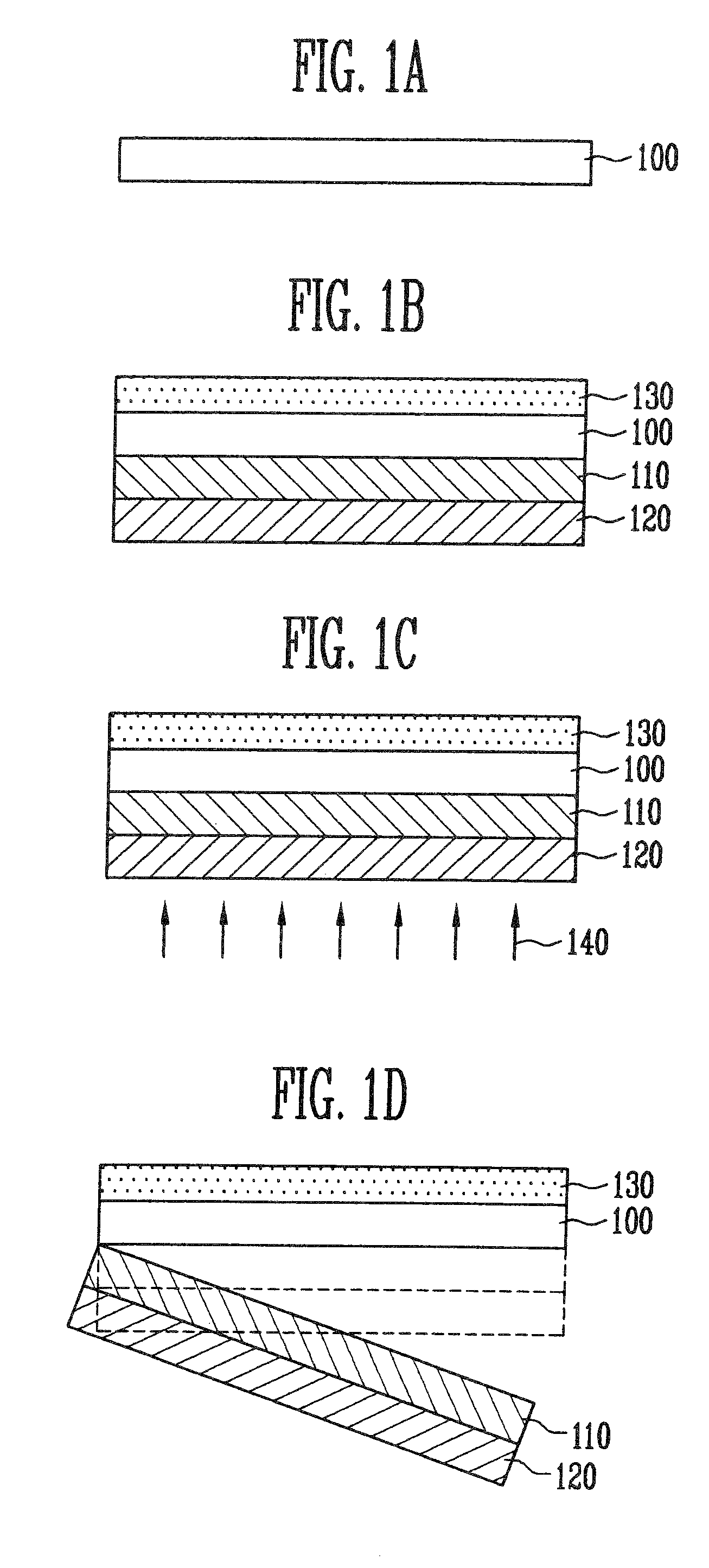
embodiment 1
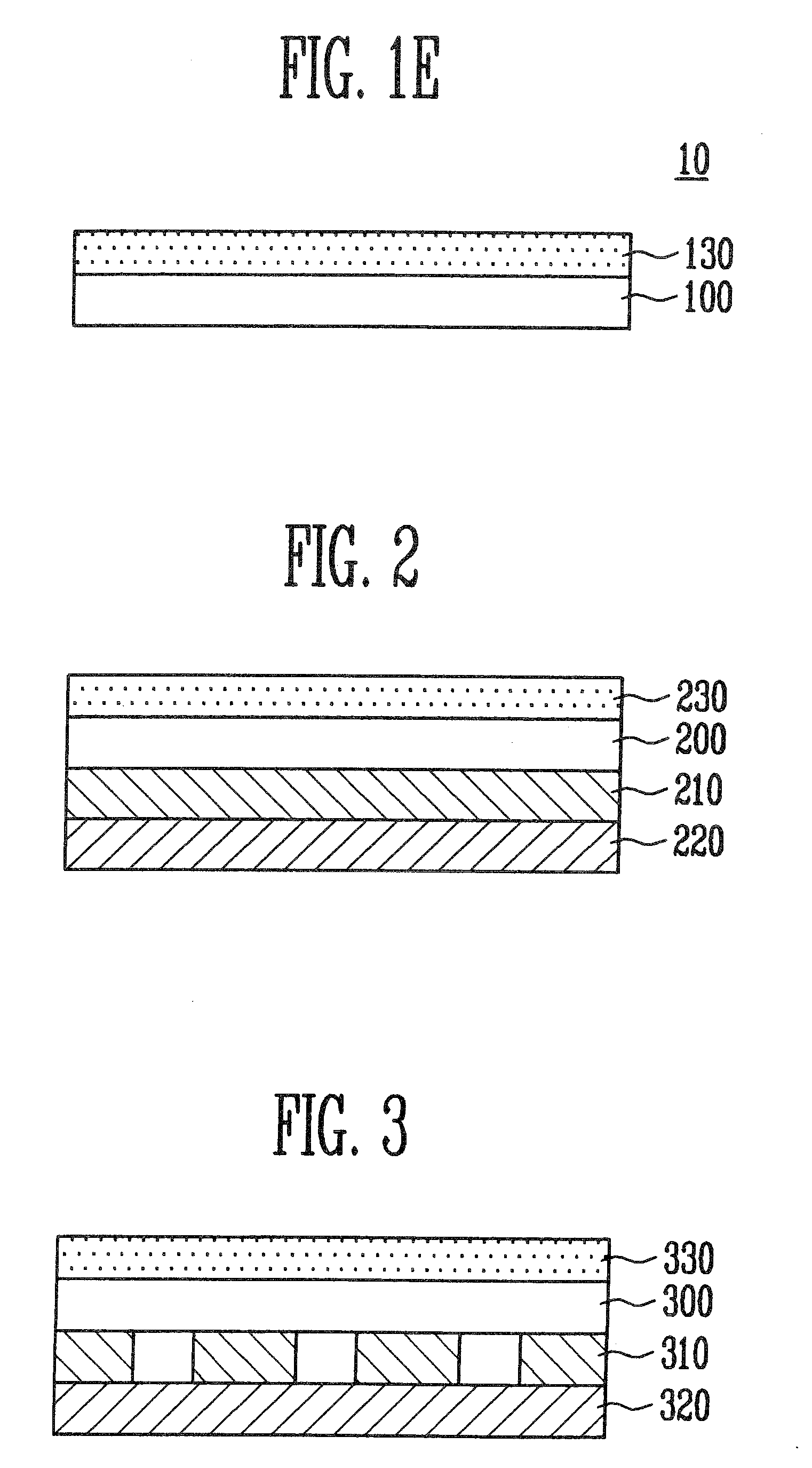
[0030]Referring to FIG. 2, in order to manufacture a device 230 on a flexible substrate 200, a sacrificial layer 210 and a substrate support 220 are formed beneath the flexible substrate 200 as shown in FIG. 2. The sacrificial layer 210 and the substrate support 220 are formed to prevent the flexible substrate 200 from being deformed when the device 230 is formed on the flexible substrate 200.
[0031]A conventional sacrificial layer would be formed of amorphous silicon (a-si). However, if the sacrificial layer is formed of amorphous silicon, a high laser energy (about 700 to 750 mJ / cm2) is irradiated onto the sacrificial layer due to the high reflexibility of the amorphous silicon. As such, if a high laser energy is irradiated onto the sacrificial layer, a device formed above the sacrificial layer may be thermally damaged. That is, heat is conducted to the device formed on a flexible substrate, and therefore, characteristics of the device may be deteriorated. Further, if the sacrifici...
embodiment 2
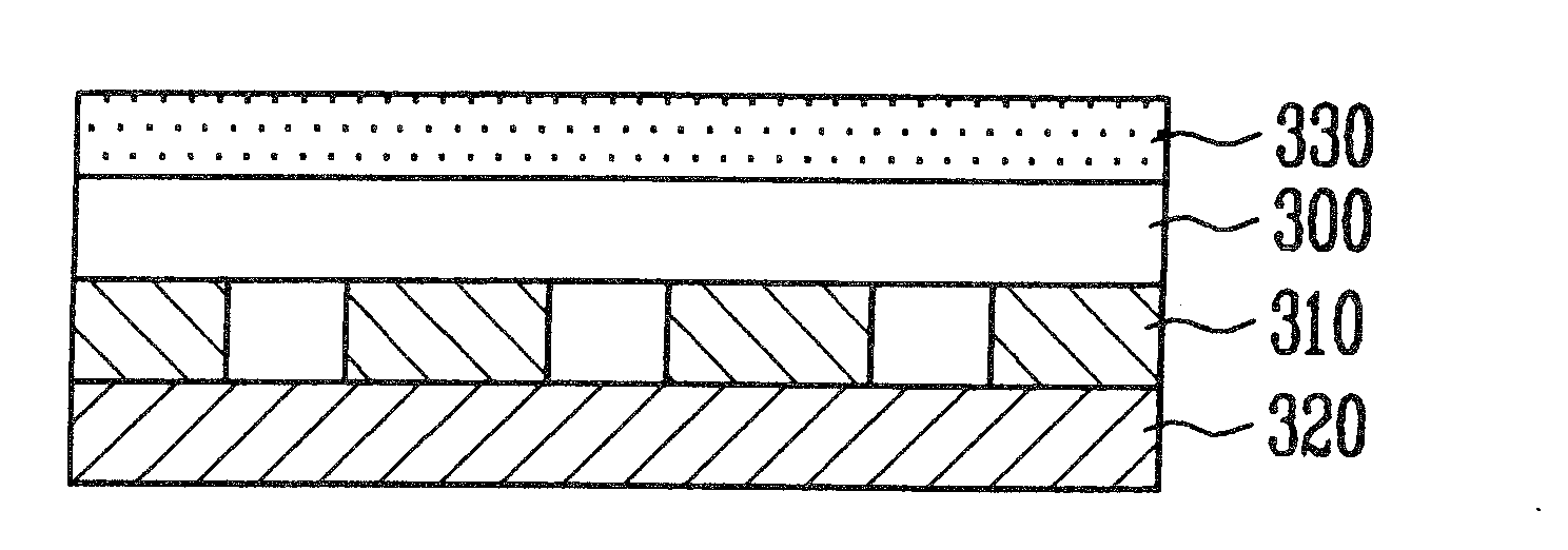
[0040]Embodiment 2 as shown in FIG. 3 is the same as Embodiment 1, except for the material of a sacrificial layer 310 and the wavelength of laser irradiated onto the sacrificial layer 310.
[0041]While a 308 nm excimer laser can be irradiated onto a conventional sacrificial layer formed of amorphous silicon. However, the 308 nm excimer laser has high maintenance cost and high price. Accordingly, in this embodiment, the laser is irradiated onto the sacrificial layer 310 using 1064 nm Nd:YAG with low maintenance cost and low price.
[0042]However, if the laser is irradiated onto the sacrificial layer 310 formed of amorphous silicon using the 1064 nm Nd:YAG, the laser having a wavelength of 1064 nm is not sufficiently absorbed into the amorphous silicon. Therefore, the sacrificial layer 310 is not entirely detached from a flexible substrate 300.
[0043]Accordingly, the sacrificial layer 310 with a high absorptivity of laser having a wavelength of 1064 nm is provided in Embodiment 2. A materi...
PUM
 Abstract
Description
Claims
Application Information