Hermetic sealing cap, electronic component accommodation package, and method for producing hermetic sealing cap
a technology of electronic components and hermetic sealing caps, which is applied in the direction of electrical apparatus casings/cabinets/drawers, soldering apparatus, and semiconductor/solid-state device details. it can solve the problem of suppressing the complexity of the production process of hermetic sealing caps
- Summary
- Abstract
- Description
- Claims
- Application Information
AI Technical Summary
Benefits of technology
Problems solved by technology
Method used
Image
Examples
first embodiment
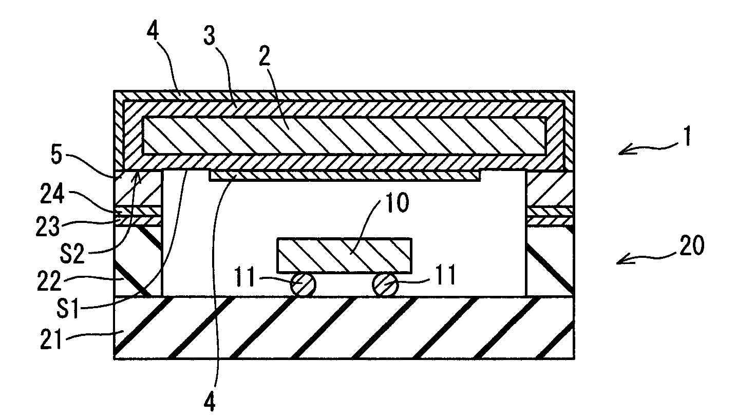
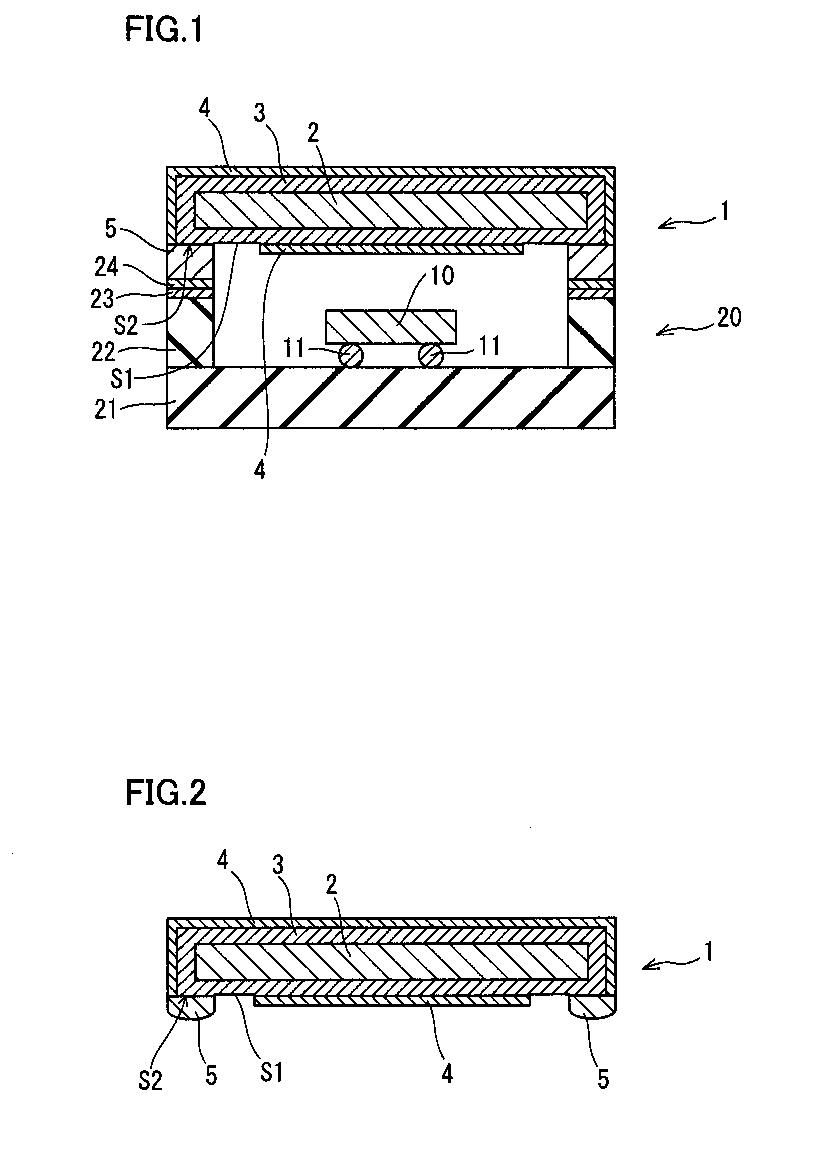
[0045]The structure of an electronic component accommodation package according to a first embodiment is first described with reference to FIG. 1.
[0046]As shown in FIG. 1, the electronic component accommodation package according to the first embodiment of the present invention is composed of a hermetic sealing cap 1, an electronic components 10 such as a quartz resonator, and an electronic component accommodation member 20 for accommodating the electronic component 10. This electronic component accommodation member 20 includes a ceramic substrate 21 that is composed of an insulating material such as alumina, and a ceramic frame 22 that provides accommodation space on a prescribed area of the surface of the ceramic substrate 21 and is formed of an insulating material such as alumina. In addition, the electronic component 10 is mounted via bumps 11 on the ceramic substrate 21 that is located in the accommodation space that is enclosed by the ceramic frame 22. Additionally, a tungsten l...
examples
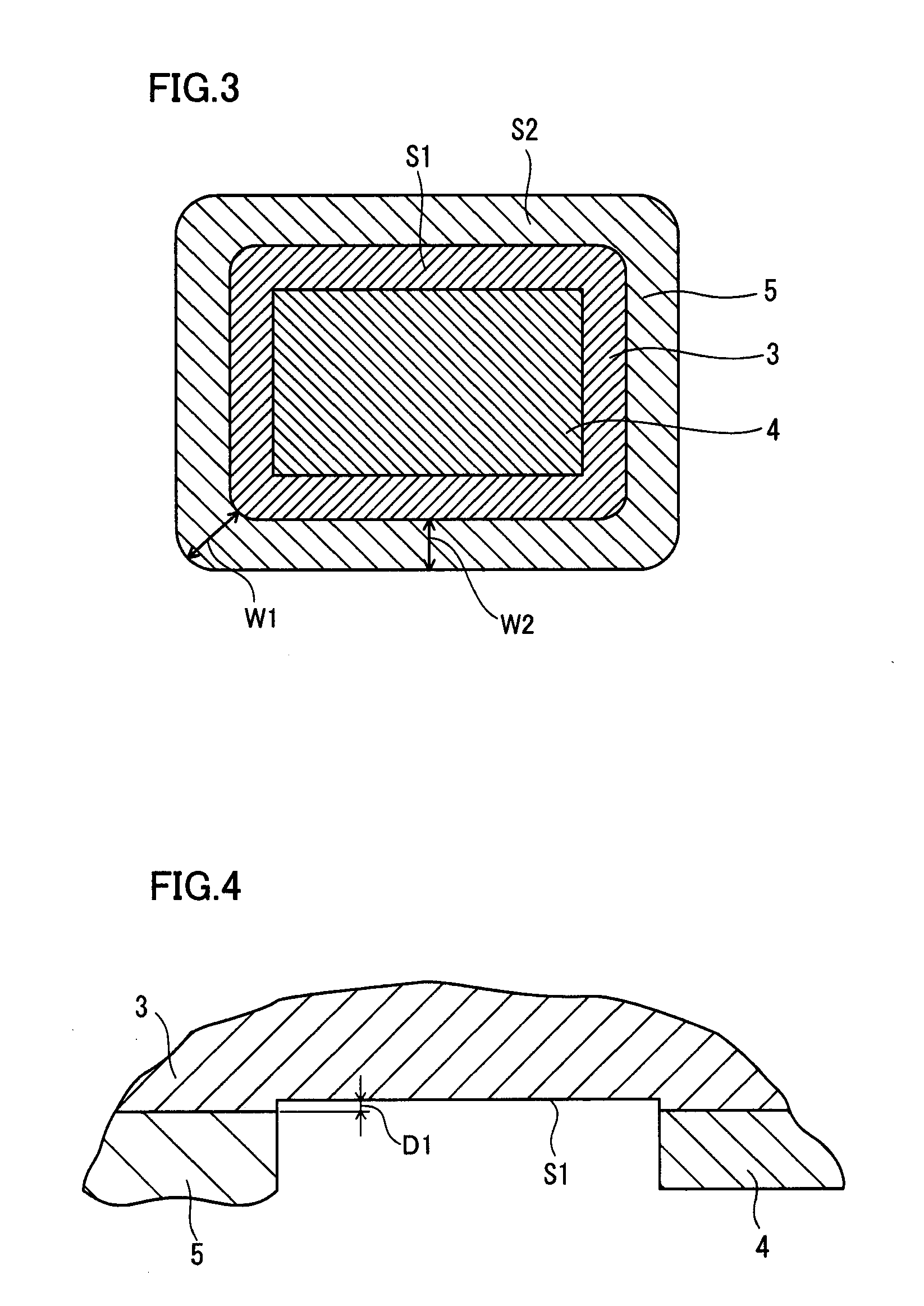
[0059]A comparative experiment is now described which has been conducted to confirm an effect of the hermetic sealing cap 1 according to the foregoing first embodiment. The comparative experiment is first described which has measured the widths and thicknesses of the solder layer before the hermetic sealing cap 1 is hermetically sealed. In this comparative experiment, samples according to examples 1 to 3 corresponding to the first embodiment, and a sample according to comparative example 1 were produced.
[0060]The samples according to the examples 1 to 3 were produced by using a production process similar to the hermetic sealing cap 1 according to the foregoing first embodiment. In addition, the samples according to the examples 1 to 3 were produced by using the ring-shaped solder 5a with thicknesses of about 0.025 mm, about 0.030 mm, and about 0.038 mm, respectively. On the other hand, dissimilarly to the foregoing first embodiment, the sample according to the comparative example 1 ...
second embodiment
[0068]With reference to FIGS. 1 and 19, in this second embodiment, the case where the shape of the area where the solder layer is formed is modified is described.
[0069]In the electronic component accommodation package according to the second embodiment of the present invention, similarly to the foregoing first embodiment, a hermetic sealing cap 30 (see FIG. 19) is joined on the upper surface of the ceramic frame 22 of the electronic component accommodation member 20 (see FIG. 1). In addition, the other parts of the electronic component accommodation package according to the second embodiment are similar to the foregoing first embodiment.
[0070]The structure of the hermetic sealing cap 30 according to the second embodiment of the present invention is now described with reference to FIG. 19. In the hermetic sealing cap 30 according to the second embodiment of the present invention, similarly to the foregoing first embodiment, in an oxidized area S5, an Au plating layer 32 is removed so...
PUM
| Property | Measurement | Unit |
|---|---|---|
| thickness | aaaaa | aaaaa |
| depth D1 | aaaaa | aaaaa |
| width | aaaaa | aaaaa |
Abstract
Description
Claims
Application Information


