Nonvolatile semiconductor storage and its manufacturing method

a manufacturing method and semiconductor technology, applied in semiconductor devices, electrical devices, transistors, etc., can solve problems such as process complexity and performance degradation, and achieve the effects of reducing power consumption, facilitating integration, and improving processing efficiency

Inactive Publication Date: 2005-04-14
RENESAS ELECTRONICS CORP
View PDF13 Cites 48 Cited by
  • Summary
  • Abstract
  • Description
  • Claims
  • Application Information

AI Technical Summary

Benefits of technology

[0010] Still further, in the nonvolatile semiconductor memory device in which the performance deterioration of the transistors in the peripheral circuit area due to tantalum does not become a problem, it became clear that no use of tantalum pentoxidxe in the peripheral circuit area made the process more complicated.
[0011] One object of the present invention is to implement a flash memory with higher integration, a higher operating speed, lower power consumption, and higher reliability, by applying tantalum pentoxide, which has a dielectric constant several times as large as that in its amorphous phase or its lower dielectric constant phase, to an inter-poly silicon insulator film of a flash memory cell.
[0012] Other object of the present invention is to implement a low cost flash memory by applying the inter-poly silicon insulator film to a peripheral circuit area as well, thereby simplifying the process.
[0013] According to one aspect of the present invention, the inter-poly silicon insulator film formed between the floating gate and the control gate was constituted from a multilayer film including at least three layers comprising a first silicon dioxide layer, a layer having nitrogen and silicon employed as main constituent elements, and a tantalum pentoxide layer. With this configuration, tantalum pentoxide can be crystallized to a high dielectric constant phase, and leakage current can also be reduced.

Problems solved by technology

Study of inventors revealed that tantalum, which is a constituent element of tantalum pentaoxide, is notably diffused into transistors in the peripheral circuit area during annealing after its deposition, thereby causing performance deterioration.
Still further, in the nonvolatile semiconductor memory device in which the performance deterioration of the transistors in the peripheral circuit area due to tantalum does not become a problem, it became clear that no use of tantalum pentoxidxe in the peripheral circuit area made the process more complicated.

Method used


Image

  • Nonvolatile semiconductor storage and its manufacturing method
  • Nonvolatile semiconductor storage and its manufacturing method
  • Nonvolatile semiconductor storage and its manufacturing method

Examples


first embodiment

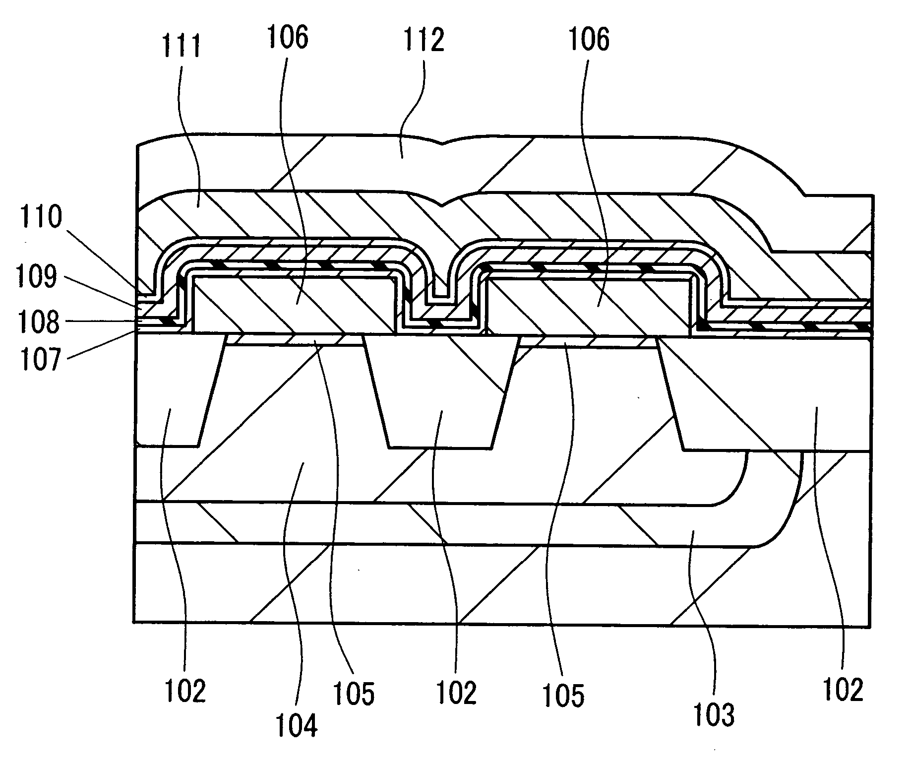
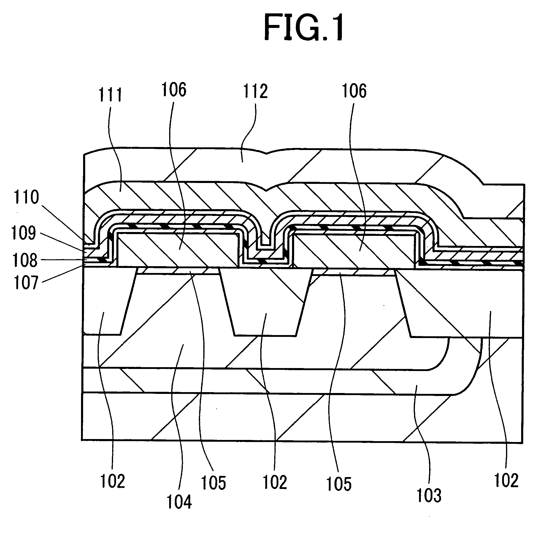
[0058] In this embodiment, an example is disclosed in which, by avoiding exposure of gate insulator films of transistors in a peripheral circuit and interfaces with silicon at the time of deposition of tantalum pentoxide of an ONTO structure and performing crystallization in a state where they were covered with poly silicon, a characteristic such as leakage current was improved at the standby time of the transistors in the peripheral circuit. This embodiment is the example where a memory cell configuration popularly called as an NOR type was adopted.

[0059] Main portions of manufacturing steps of a nonvolatile semiconductor memory device in this embodiment are shown in FIGS. 10A to 10F and FIGS. 11A to 11D. The nonvolatile semiconductor memory device is broadly classified into: [0060] (1) a memory array area in which memory cells are disposed in an array; and [0061] (2) a peripheral circuit area that functions to make memory cell selection and information reading and writing. The pe...

second embodiment

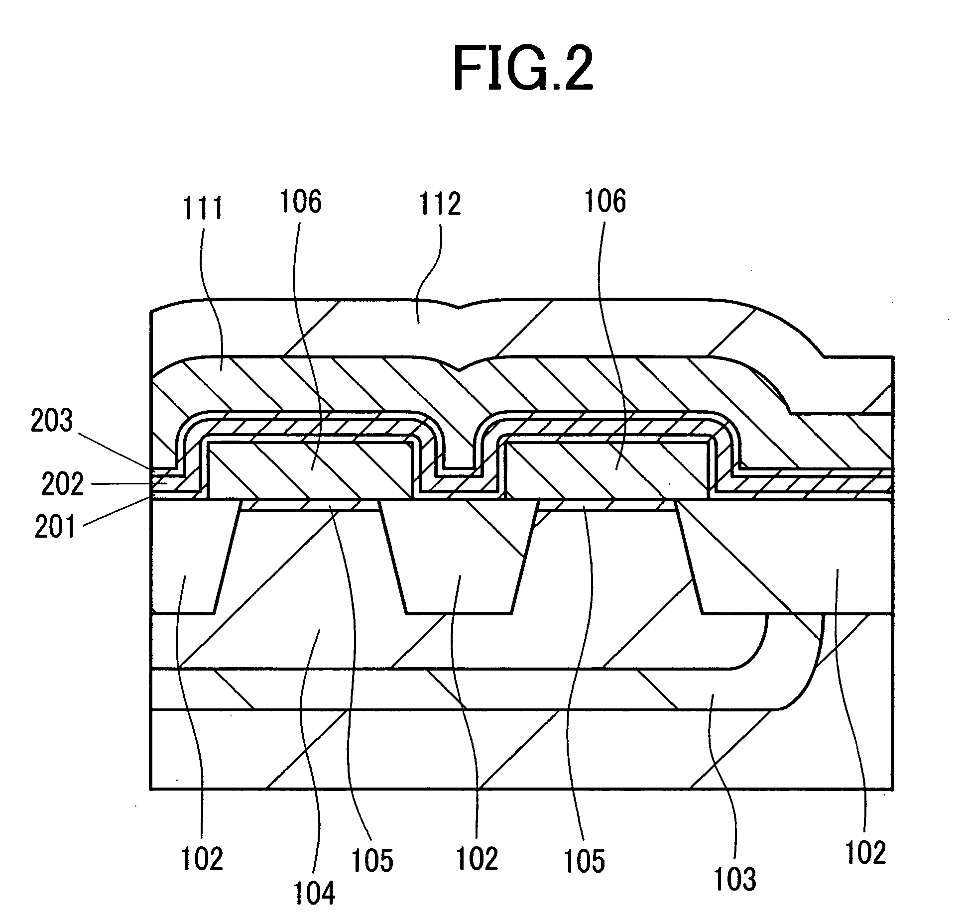
[0080] In this embodiment, other embodiment is disclosed in which by avoiding exposure of the gate insulator films of the transistors in the peripheral circuit and the interfaces with silicon at the time of deposition of the tantalum pentoxide film of the ONTO structure and performing crystallization in a state where they are covered with poly silicon, the characteristic such as leakage current at the standby time of the transistors in the peripheral circuit was improved. This embodiment is the example in which a memory cell configuration popularly called as an AND type was adopted.

[0081] Main portions of manufacturing steps of a nonvolatile semiconductor memory device in this embodiment are shown in FIGS. 12A to 12F and FIGS. 13A to 13F, and FIGS. 14A to 14D. As in the first embodiment, the memory array area, peripheral circuit area, high-voltage devices, and low voltage devices were displayed with the arrows on top. Further, as in the first embodiment, sections of the memory arra...

third embodiment

[0103] In this embodiment, other embodiment is disclosed in which by avoiding exposure of the gate insulator films of the transistors in the peripheral circuit and the interfaces with silicon at the time of deposition of tantalum pentoxide of the ONTO structure and performing crystallization in a state where they are covered with poly silicon, the characteristic such as leakage current at the standby time of the transistors in the peripheral circuit was improved. In this embodiment, third gates that are different from the floating gates and the control gates, (which will be hereinafter referred to as assist gates), are disposed in the memory array area, thereby separating the memory cells.

[0104] Main portions of manufacturing steps of a nonvolatile semiconductor memory device in this embodiment are shown in FIGS. 15A to 15F and FIGS. 16A to 16F, and FIGS. 17A to 17C. As in the first embodiment, the memory array area, peripheral circuit area, high voltage devices, and low voltage de...


PUM

PropertyMeasurementUnit
thicknessaaaaaaaaaa
thicknessaaaaaaaaaa
thicknessaaaaaaaaaa

Abstract

To achieve a higher operating speed, higher reliability, and lower power consumption by reducing the thickness of an inter-poly silicon insulator film between a floating gate and a control gate of a flash memory, a silicon dioxide film, a silicon nitride film, tantalum pentoxide, and a silicon dioxide film are formed in a multilayer structure to serve as the inter-poly insulator film between a floating gate and a control gate. With this configuration, tantalum pentoxide formed on the silicon nitride film has a dielectric constant of 50 or more, which is higher than that of the silicon dioxide film, and the thickness of the inter-poly silicon insulator film can be reduced.

Description

TECHNICAL FIELD [0001] The present invention relates to a nonvolatile semiconductor memory device and its manufacturing method. More specifically, the invention relates to a technique that can achieve miniatuarization, higher integration, a higher operating speed, and high reliability. BACKGROUND ART [0002] Miniatuarization and high integration of nonvolatile memories with their floating gates introduced into gate insulator film multilayer structures of MOS transistors are easy, because of their simple structure. Thus, the nonvolatile memory becomes a standard nonvolatile memory cell structure in a silicon integrated circuit. Flash memories, in particular, which have enabled electrical bulk erasing, are suitable for implementation of small-sized, large-capacity nonvolatile semiconductor memory devices. Thus, taking the flash memory as the memory that is essential for portable information devices, development efforts toward a larger capacity, a higher operating speed, lower power con...

Claims


Application Information

Patent Timeline
Patent Type & Authority Applications(United States)
IPC IPC(8): H01L21/28H01L21/8247H01L27/105H01L27/115H01L29/51H01L29/788H01L29/792
CPCH01L21/28211H01L27/105H01L29/511H01L27/11526H01L27/11546H01L27/115H10B41/49H10B41/40H10B69/00
Inventor MIKI, HIROSHI
Owner RENESAS ELECTRONICS CORP
Why Eureka
Try Eureka