Wired circuit board and electronic device

a wired circuit board and electronic device technology, applied in the direction of cross-talk/noise/interference reduction, coupling device connection, electrical apparatus casing/cabinet/drawer, etc., can solve the problem of signal wiring being broken under such stress, transmission loss in the conductor layer (line), and difficulty in preventing a breakage of the conductive layer. , to achieve the effect of excellent long-term reliability

Inactive Publication Date: 2009-12-10
NITTO DENKO CORP
View PDF8 Cites 5 Cited by
  • Summary
  • Abstract
  • Description
  • Claims
  • Application Information

AI Technical Summary

Benefits of technology

[0010]With the wiring board described in U.S. Pat. No. 6,353,189 and the connector described in U.S. Pat. No. 4,926,007, a transmission loss in the conductor layer (line) can be reduced, but it is difficult to prevent a broken line in the conductive layer due to the stress and to reduce the transmission loss at the same time.
[0011]It is therefore an object of the present invention to provide a wired circuit board which allows the prevention of a transmission loss in a signal wiring as well as a relief in the stress received when a first casing and a second casing are relatively rotated and an electronic device using the wired circuit board.
[0013]The wired circuit board comprises the ground layer formed to surround each of the signal wirings in the perpendicular direction to the longitudinal direction. Accordingly, even when a signal transmitted by each of the signal wirings is increased in frequency, the transmission loss in the signal wiring can be reduced. In addition, the slit along the longitudinal direction is formed between the signal wirings in the insulating layer. Therefore, even when the wired circuit board receives a stress that distorts the wired circuit board in the perpendicular direction to the longitudinal direction and to the thickness direction, such a stress can be relieved by the slit. As a result, it is possible to effectively prevent damage such as a broken wiring in the conductive layer due to such a stress to ensure excellent long-term reliability.
[0015]In the wired circuit board, the slit is extensively formed adjacent to each of the connecting terminals on one side in the longitudinal direction, and adjacent to each of the connecting terminals on the other side in the longitudinal direction. As a result, it is possible to more reliably relieve the stress mentioned above, while the strength of the entire wired circuit board is secured.
[0017]In the electronic device, each of the signal wirings is disposed around the connecting member and is arranged parallel along a direction in which the first casing and the second casing relatively rotate. As a result, when the first casing and the second casing are relatively rotated by the connecting member, the wired circuit board receives a stress that twists the wired circuit board in the direction in which the first casing and the second casing relatively rotate, i.e., in the direction in which each of the signal wirings is arranged parallel, more specifically in the perpendicular direction to the longitudinal direction and thickness direction of the wired circuit board and distorted in the perpendicular direction to the longitudinal direction and to the thickness direction. However, such a stress can be relieved by the slit. Therefore, it is possible to relatively rotate the first casing and the second casing smoothly by the connecting member and prevent damage such as a broken wiring in the wired circuit board at the connecting member to ensure excellent long-term reliability.

Problems solved by technology

As a result, a signal wiring may be broken under such a stress.
With the wiring board described in U.S. Pat. No. 6,353,189 and the connector described in U.S. Pat. No. 4,926,007, a transmission loss in the conductor layer (line) can be reduced, but it is difficult to prevent a broken line in the conductive layer due to the stress and to reduce the transmission loss at the same time.

Method used


Image

  • Wired circuit board and electronic device
  • Wired circuit board and electronic device
  • Wired circuit board and electronic device

Examples


example 1

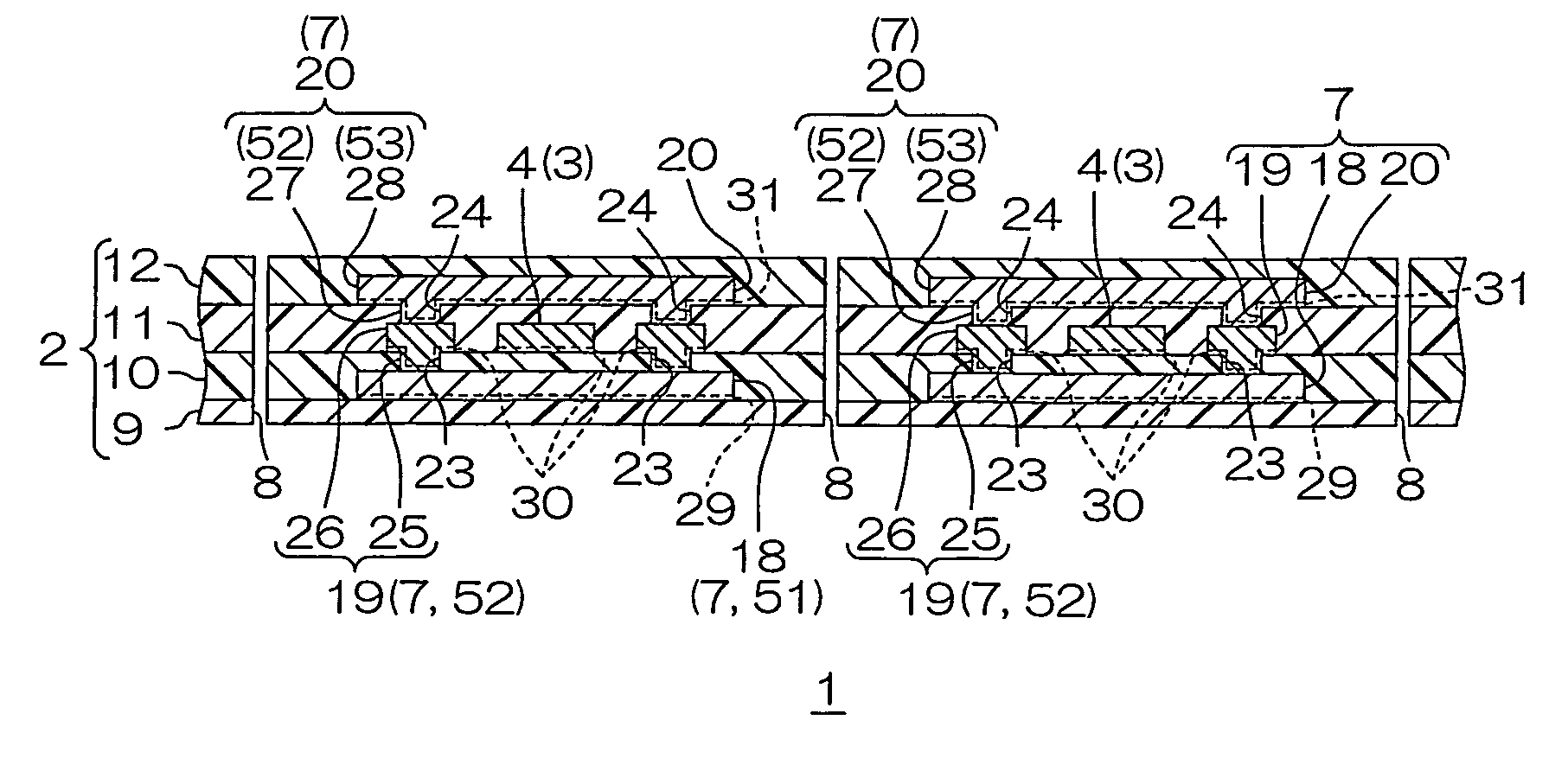
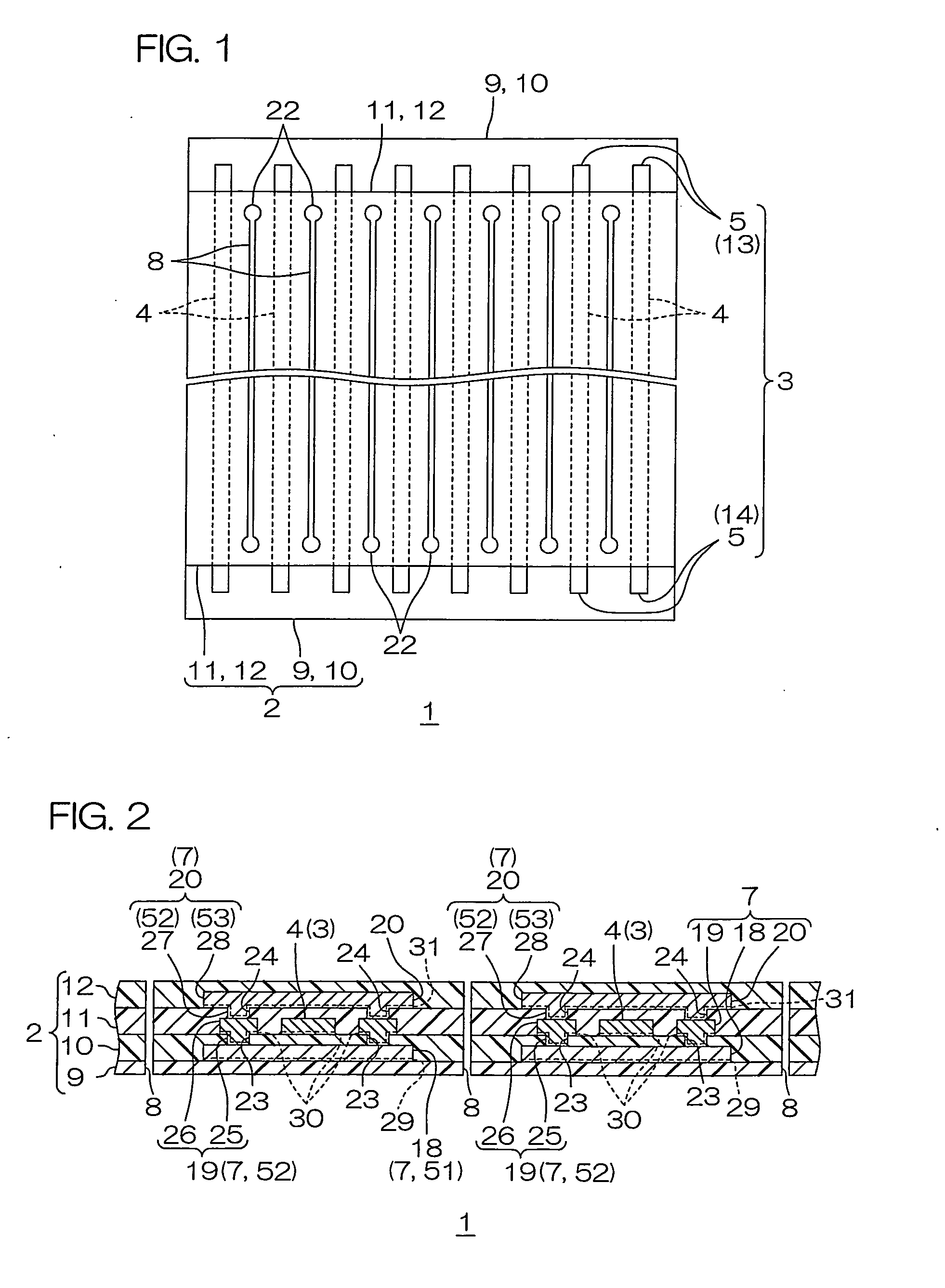
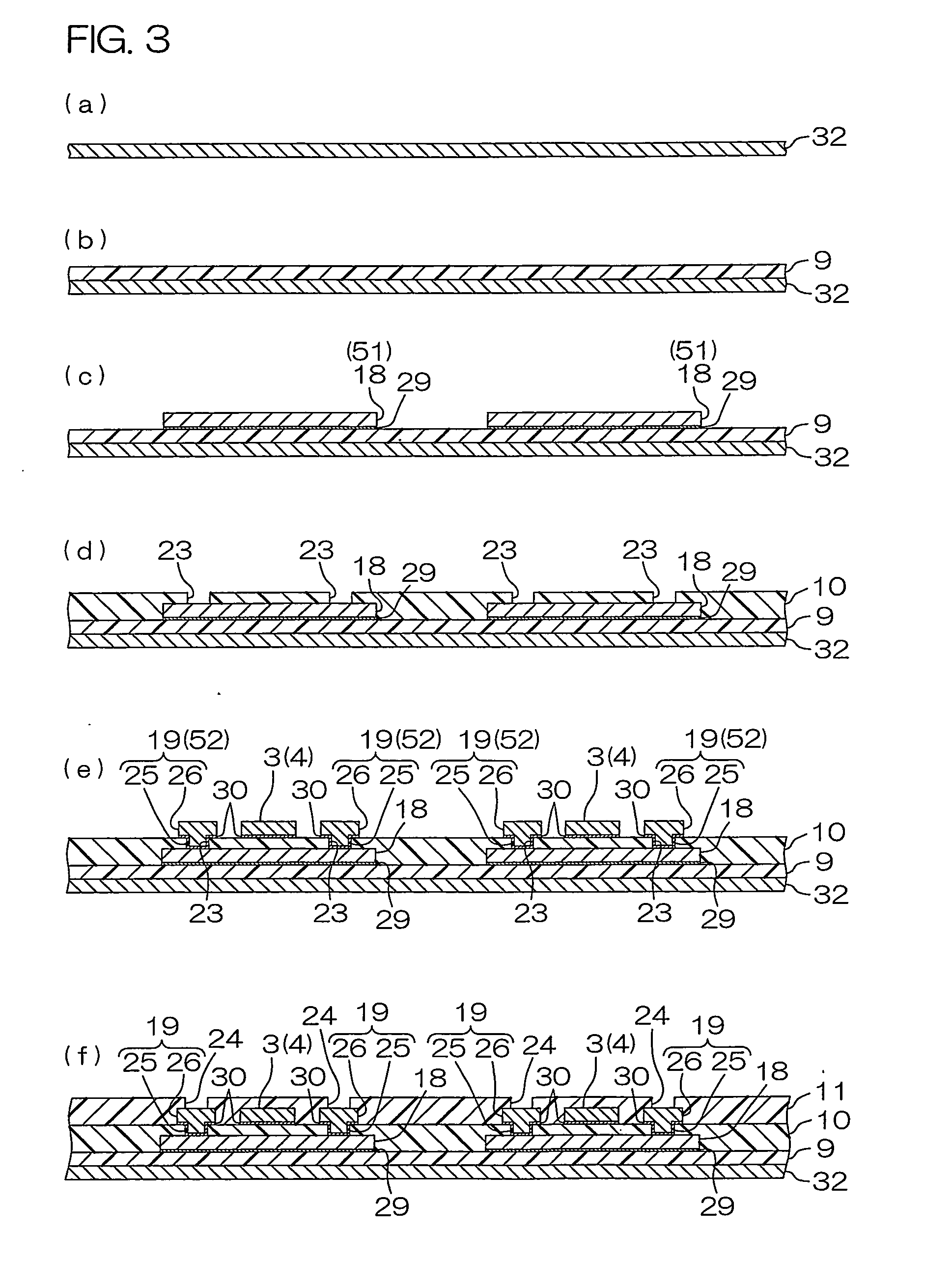
[0185]A metal supporting board made of stainless steel having a thickness of 20 μm was prepared (see FIG. 3(a)). Then, a varnish of a photosensitive polyamic acid resin was coated on the upper surface of the metal supporting board, dried, exposed to light via a photomask, developed, and cured by heating to form a first insulating layer made of polyimide having a thickness of 12 μm on the metal supporting board (see FIG. 3(b)).

[0186]Next, a chromium thin film having a thickness of 0.03 μm and a copper thin film having a thickness of 0.07 μm, each as a first metal thin film, were successively formed on the upper surface of the first insulating layer by chromium sputtering and copper sputtering. Subsequently, a plating resist was formed in a pattern reverse to the pattern of first ground layers on the upper surface of the first metal thin film. Then, in accordance with an additive method, the first ground layers (lower ground layers) each made of copper having a thickness of 12 μm and ...


PUM


Abstract

A wired circuit board has an insulating layer extending in a longitudinal direction, a conductive layer having a plurality of signal wirings covered with the insulating layer and arranged in mutually spaced-apart and parallel relation in a perpendicular direction to the longitudinal direction and a thickness direction of the insulating layer, and connecting terminals provided on both longitudinal ends of each of the signal wirings and exposed from the insulating layer, and a ground layer covered with the insulating layer and formed to surround each of the signal wirings in a perpendicular direction to the longitudinal direction. A slit along the longitudinal direction is formed between each of the signal wirings in the insulating layer.

Description

CROSS-REFERENCE TO RELATED APPLICATION[0001]The present application claims priority from Japanese Patent Application No. 2006-271035 filed on Oct. 2, 2006, the contents of which are herein incorporated by reference in their entirety.BACKGROUND OF THE INVENTION[0002]1. Field of the Invention[0003]The present invention relates to a wired circuit board and an electronic device and, more particularly, to a wired circuit board such as a flexible wired circuit board and an electronic device using the wired circuit board, such as a cellular phone.[0004]2. Description of the Related Art[0005]Conventionally, flexible wired circuit boards have been used in the movable members of various electronic devices such as a cellular phone, a notebook personal computer, and a video camera.[0006]In recent years, in terms of higher data density, an increase in the frequency of a signal has been required in such a flexible wired circuit board. However, when the frequency of the signal is increased, a tran...

Claims


Application Information

Patent Timeline
Patent Type & Authority Applications(United States)
IPC IPC(8): H05K5/00
CPCH05K1/0219H05K1/0271H05K1/028H05K2201/09809H05K2201/09063H05K2201/09236H05K2201/09563H05K1/148
Inventor HU, SZU-HANHO, VOON YEEYAMAZAKI, HIROSHIMCCASLIN, MARTIN JOHN
Owner NITTO DENKO CORP
Why Eureka
Try Eureka