High-speed PCB and difference via hole impedance control method

A technology of PCB board and via hole, which is applied to the formation of electrical connection of printed components, electrical connection of printed components, printed circuit components, etc., can solve problems such as reducing the performance of high-speed PCBs, reducing the performance of electronic products, and discontinuous impedance of transmission lines.

Active Publication Date: 2013-08-21
GUANGZHOU FASTPRINT CIRCUIT TECH
View PDF4 Cites 40 Cited by
  • Summary
  • Abstract
  • Description
  • Claims
  • Application Information

AI Technical Summary

Problems solved by technology

Vias may exhibit discontinuities in transmission line impedance on the transmission line, causing signal reflections that degrade signal integrity
At this stage, the research on high-speed PCB vias has not fully considered the factors that affect the impedance of the vias. The theoretical impedance of the vias in the designed high-speed PCB is quite different from the actual one, which reduces the performance of high-speed PCBs, thereby reducing the performance of electronic products. performance

Method used


Image

  • High-speed PCB and difference via hole impedance control method
  • High-speed PCB and difference via hole impedance control method
  • High-speed PCB and difference via hole impedance control method

Examples


Embodiment 1

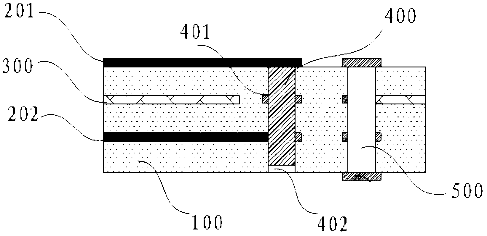
[0028] refer to figure 1 , 2 , in an embodiment of the high-speed PCB board of the present invention, a high-speed PCB board includes an insulating layer 100, a circuit layer, and a reference layer 300, and a differential transmission line 203 is arranged in the circuit layer, and the circuit layer includes a circuit layer arranged on the insulating layer 100. The outer outer circuit layer 201 and the inner circuit layer 202 arranged in the insulating layer 100, the reference layer 300 is arranged between the inner circuit layer 202 and the outer circuit layer 201, the reference layer 300 is provided with an anti-pad 301, and the differential transmission line 203 of each circuit layer is connected through a via hole 400, and a ground shielding hole 500 is provided around the via hole 400, and the via hole 400 is connected between the reference layer 300 and the inner layer circuit layer. A pad is provided at the position 202 , and a stub 402 is provided in the via hole 400 ....

Embodiment 2

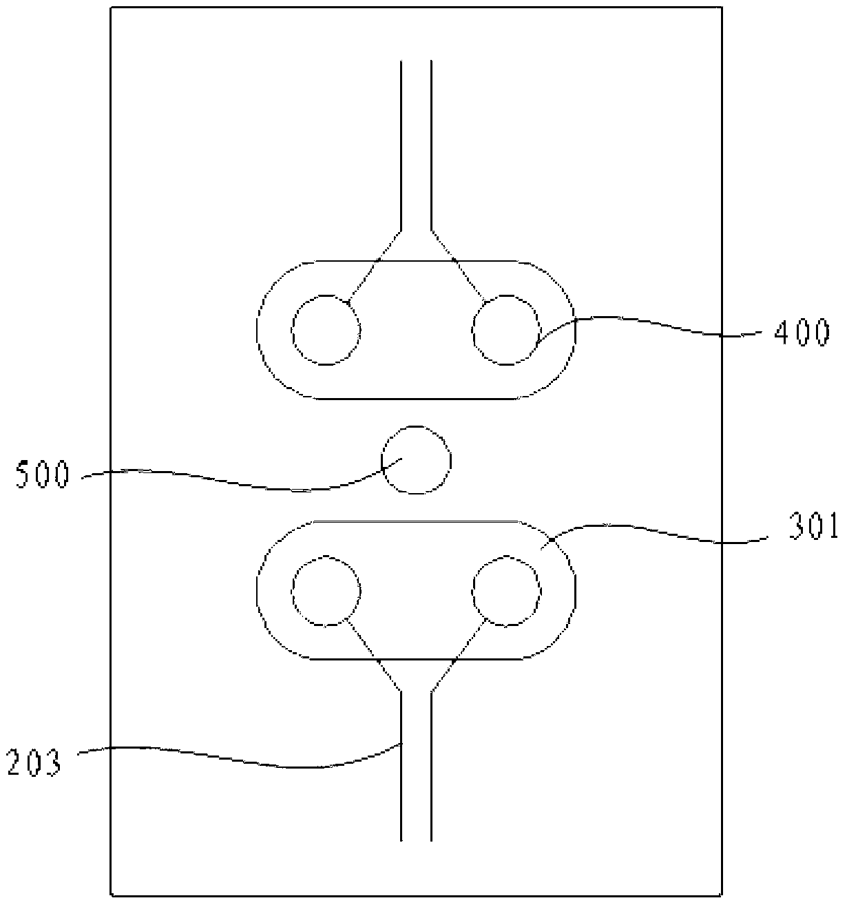
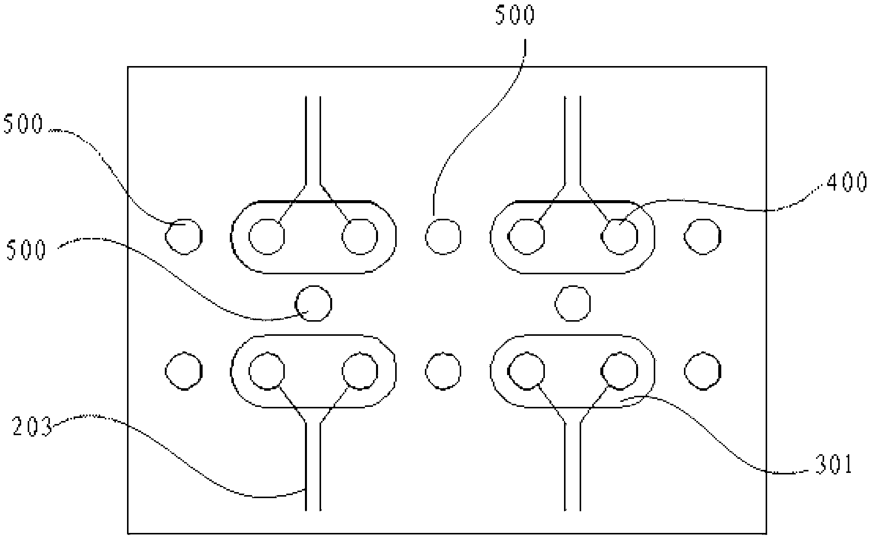
[0031] Such as image 3 As shown, there are three ground shielding holes 500 . The three ground shielding holes 500 are arranged in a triangle around the via hole 400 .

[0032] When the signal passes through the via hole 400, coupling will occur, thereby reducing the integrity of the signal. By setting the ground shielding hole 500 around the via hole 400, the coupling of the via hole can be reduced, thereby reducing the transmission loss of the via hole 400 and improving the integrity of the signal. , the non-connection pads 401 and stubs 402 will affect the impedance of the via hole 400, and the impedance of the via hole 400 can be compared with the impedance of the differential transmission line 203 through a suitable number of non-connection pads 401 and short columns 402 of a suitable size. Consistent, thereby reducing signal reflection and improving signal integrity.

[0033] A controllable design method for differential via impedance of high-speed PCB board:

[0034...


PUM


Abstract

The invention discloses a high-speed PCB which comprises an insulating layer, line layers and a reference layer. A difference transmission line is arranged in each line layer. Each line layer comprises an outer layer line layer arranged outside the insulating layer and an inner layer line layer arranged inside the insulating layer. The reference layer is arranged between each inner layer line layer and each outer layer line layer. An anti-pad is arranged in the reference layer. The difference transmission lines of the line layers are communicated through via holes. Grounded screen holes are formed around the via holes and / or pads are arranged in the via holes near the reference line and the inner layer line layer and / or short columns are arranged in the via holes. The invention further discloses a design method of difference via hole impedance control of the high-speed PCB. Coupling of the via holes can be reduced by arranging the grounded screen holes around the via holes, transmission loss of the via holes is reduced, integrity of signals is improved, impedance of the via holes can be identical with impedance of the difference transmission lines through reasonable design of the via holes, reflection of the signals is reduced, and integrity of the signals is improved.

Description

technical field [0001] The invention relates to the field of electronic components, in particular to a high-speed PCB board and a differential via hole impedance control method. Background technique [0002] PCB (Printed Circuit Board) board, also known as printed circuit board, is an important electronic component, a support for electronic components, and a provider of electrical connections for electronic components. High-speed PCB boards are widely used as the carrier of high-tech value-added electronic components. Nowadays, the design of high-tech value-added electronic products is pursuing low loss, high reliability, miniaturization, etc., and one of the key factors is It is the design of the via hole in the PCB board. [0003] In a multi-layer PCB, vias are used as conductors connecting different circuit layers. At low frequencies, vias will not affect signal transmission, but when the frequency exceeds 1GHZ or the signal rise time is less than or equal to 1ns, the vi...

Claims


Application Information

Patent Timeline
Patent Type & Authority Applications(China)
IPC IPC(8): H05K1/11H05K3/42
Inventor 陈蓓王红飞曾志军
Owner GUANGZHOU FASTPRINT CIRCUIT TECH
Why Eureka
Try Eureka