Ald processing techniques for forming non-volatile resistive-switching memories
- Summary
- Abstract
- Description
- Claims
- Application Information
AI Technical Summary
Problems solved by technology
Method used
Image
Examples
process example
i. Process Example
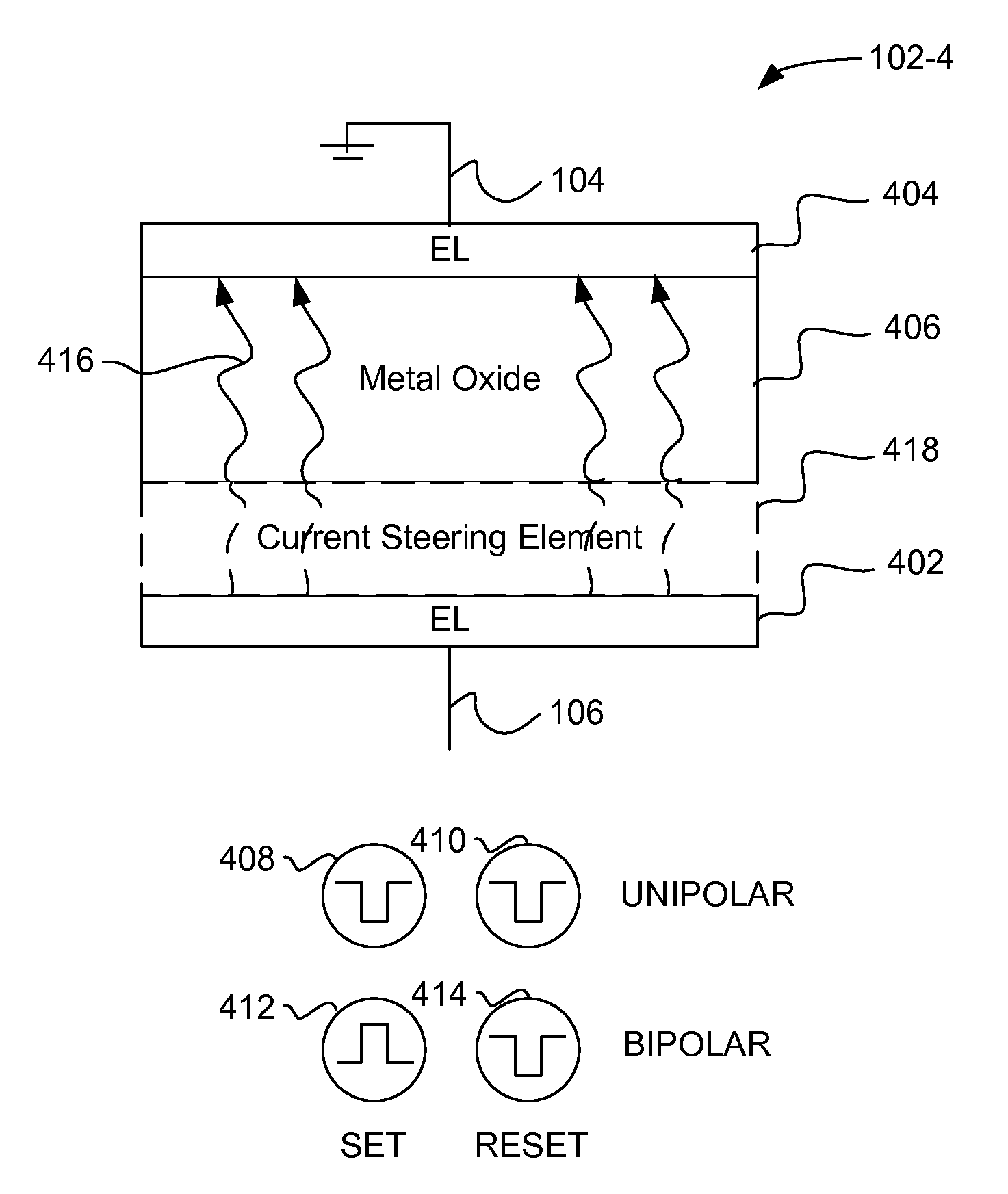
[0082]As an example, a memory element of the type of the memory element 102-4 can be formed using an aluminum oxide layer 402. A typical ALD deposition process may be performed using a purge time of 30 seconds. For the deposition of aluminum oxide, the purge time can be reduced to, for example, approximately 15 seconds (or less than 20 seconds, or in the range of 5-20 seconds, in the range of 10-17 seconds, etc.).
[0083]Without being bound by theory, and as described above, increased impurities can passivate traps in the deposited metal oxide. Shortening the purge duration can increase the number of impurities in the deposited film because less purge time results in fewer impurities being removed, thereby reducing the amount of voltage needed to form the memory elements. The shortened pulse duration should therefore reduce forming voltage regardless of the material being deposited or the precursor being used.
ii. Experimental Data
[0084]FIG. 6D is a distribution plot ...
PUM
 Abstract
Description
Claims
Application Information


