Semiconductor memory apparatus and method of controlling redundancy thereof

a memory apparatus and semiconductor technology, applied in the field of semiconductor memory apparatus, can solve problems such as increasing current consumption, and achieve the effect of controlling the redundancy of the semiconductor memory apparatus and reducing current consumption

Inactive Publication Date: 2009-12-10
SK HYNIX INC
View PDF11 Cites 1 Cited by
  • Summary
  • Abstract
  • Description
  • Claims
  • Application Information

AI Technical Summary

Benefits of technology

[0010]The embodiments of the present invention provide a semiconductor memory apparatus capable of reducing current consumption and a method of controlling redundancy of the semiconductor memory apparatus.

Problems solved by technology

However, the refresh operation is performed in a predetermined direction, that is, a row direction, not a column direction, which makes it unnecessary to operate the redundancy circuit during the refresh period.
As described above, in the semiconductor memory apparatus according to the related art, the redundancy circuit is also operated during the refresh period, which results in an increase in current consumption.

Method used


Image

  • Semiconductor memory apparatus and method of controlling redundancy thereof
  • Semiconductor memory apparatus and method of controlling redundancy thereof
  • Semiconductor memory apparatus and method of controlling redundancy thereof

Examples


Embodiment Construction

[0019]A semiconductor memory apparatus and a method of controlling redundancy thereof according to embodiments of the present invention will now be described in detail with reference to the accompanying drawings.

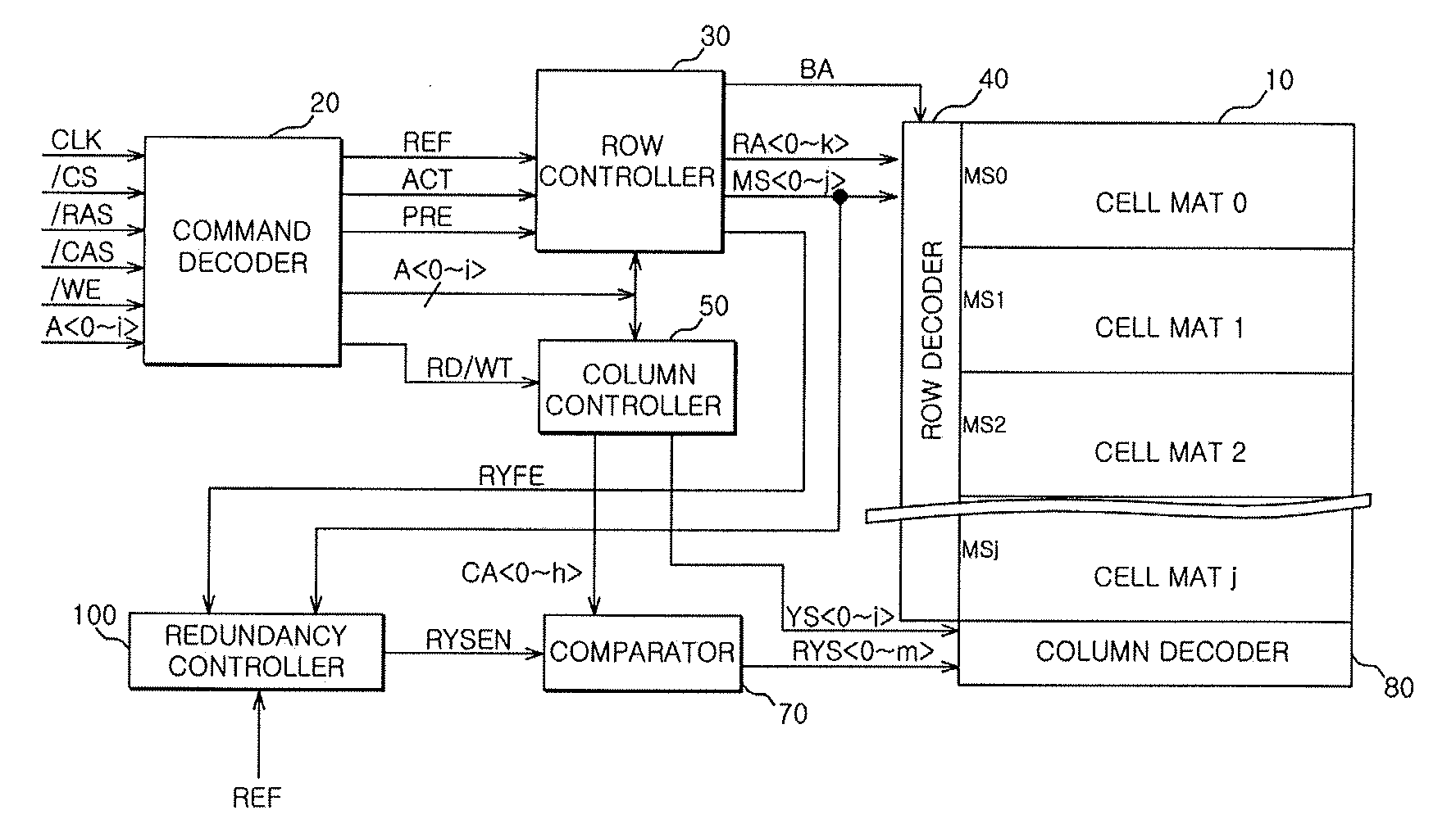
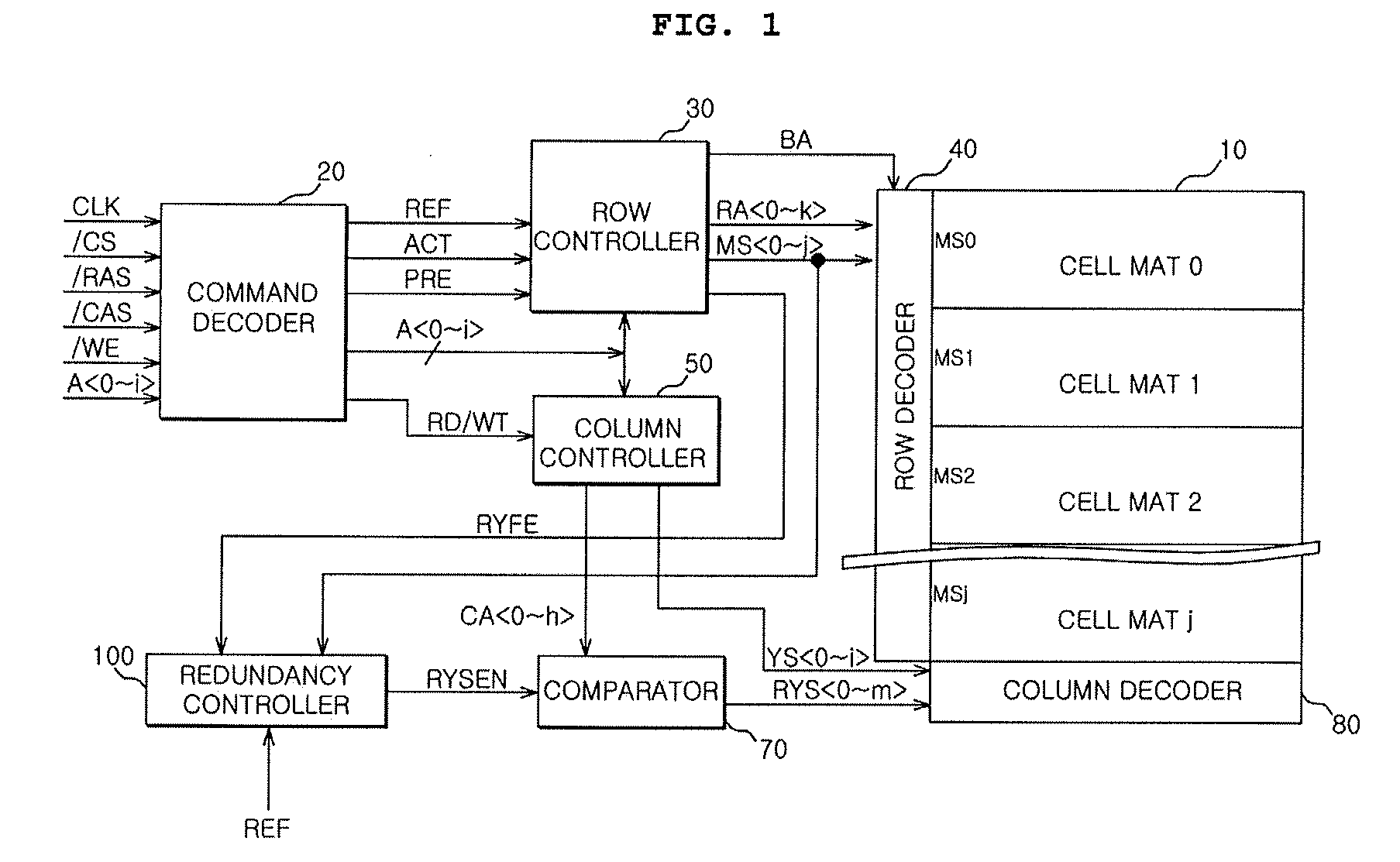
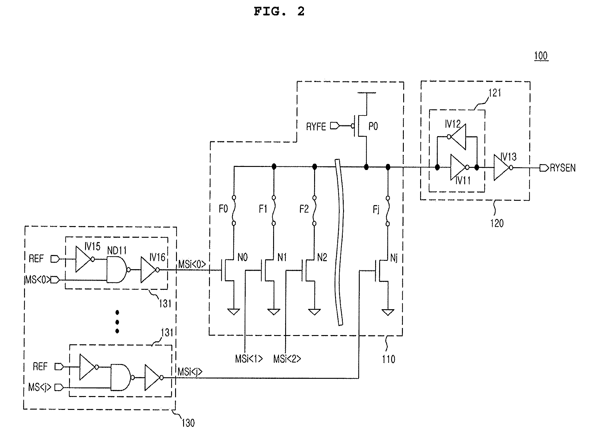
[0020]As shown in FIG. 1, a semiconductor memory apparatus according to an embodiment of the invention includes a memory cell array 10, a command decoder 20, a row controller 30, a row decoder 40, a column controller 50, a redundancy controller 100, a comparator 70, and a column decoder 80.

[0021]The memory cell array 10 is a group of memory cells arranged in a matrix. The memory cell array may be called a memory bank, and a semiconductor memory apparatus may include a plurality of memory banks according to its memory capacity. The memory cell array 10 has a plurality of small areas and a redundancy area that will be replaced with a defective area among the plurality of small areas. The small areas are arranged in a row direction and are called cell mats, which correspond to ...


PUM


Abstract

A semiconductor memory apparatus includes a memory cell array. A redundancy controller that determines whether to activate a redundancy enable signal on the basis of a refresh signal and outputs the redundancy enable signal. A comparator outputs a redundancy selection signal in response to the redundancy enable signal and an address signal. A decoder activates an area corresponding to the redundancy selection signal in the memory cell array.

Description

CROSS-REFERENCE TO RELATED PATENT APPLICATION[0001]This application is a divisional of U.S. patent application Ser. No. 11 / 822,359, filed Jul. 5, 2007, the subject matter of which application is incorporated herein by reference in its entirety.[0002]This application claims the benefit of Korean Patent Application No. 10-2006-0099709, filed on Oct. 13, 2006, in the Korean Intellectual Property Office, the disclosure of which is incorporated herein in its entirety by reference.BACKGROUND OF THE INVENTION[0003]1. Technical Field[0004]The present invention relates to a semiconductor memory apparatus, and more particularly, to a semiconductor memory apparatus having redundancy memory cells and a method of controlling redundancy thereof.[0005]2. Related Art[0006]In general, semiconductor memory apparatuses each have redundancy memory cells capable of replacing defective memory cells during a manufacturing process and a redundancy circuit for controlling the redundancy memory cells.[0007]T...

Claims


Application Information

Patent Timeline
Patent Type & Authority Applications(United States)
IPC IPC(8): G11C29/00G11C17/18G11C7/00
CPCG11C8/12G11C29/83G11C11/406G11C8/20G11C29/00
Inventor CHO, JIN HEE
Owner SK HYNIX INC
Why Eureka
Try Eureka