

System and method for modifying a data set of a photomask
a technology of photomask and data set, applied in the field of data preparation for lithography, can solve the problems of increasing the difficulty of maintaining sufficient yield, and achieve the effect of improving the scor
- Summary
- Abstract
- Description
- Claims
- Application Information
AI Technical Summary
Benefits of technology
Problems solved by technology
Method used
Image

Examples
Embodiment Construction
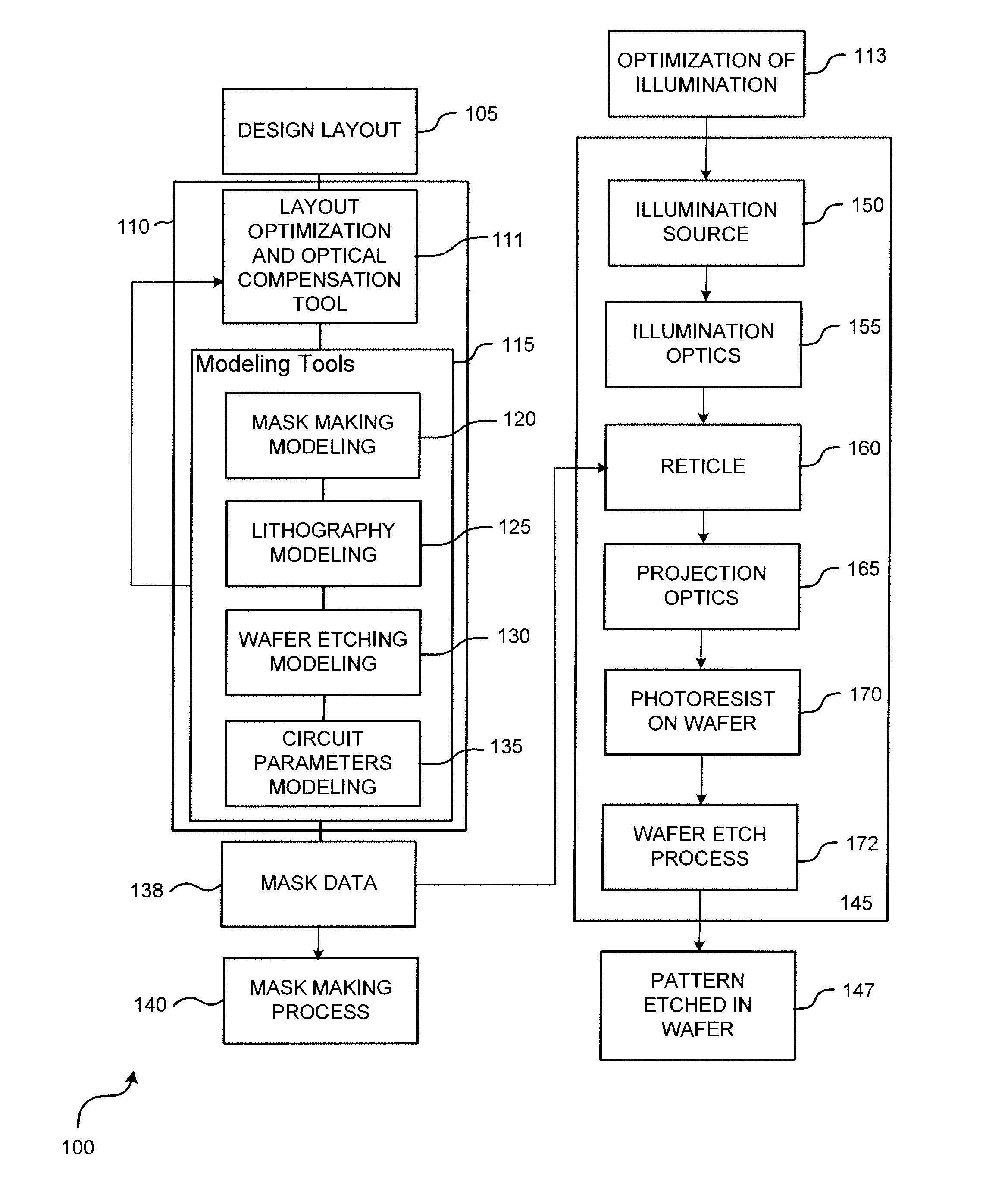
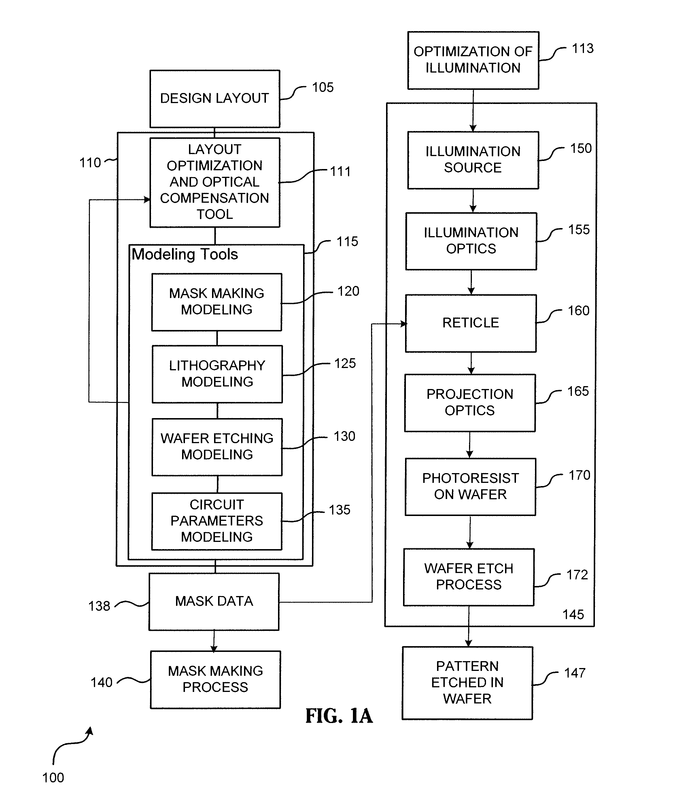
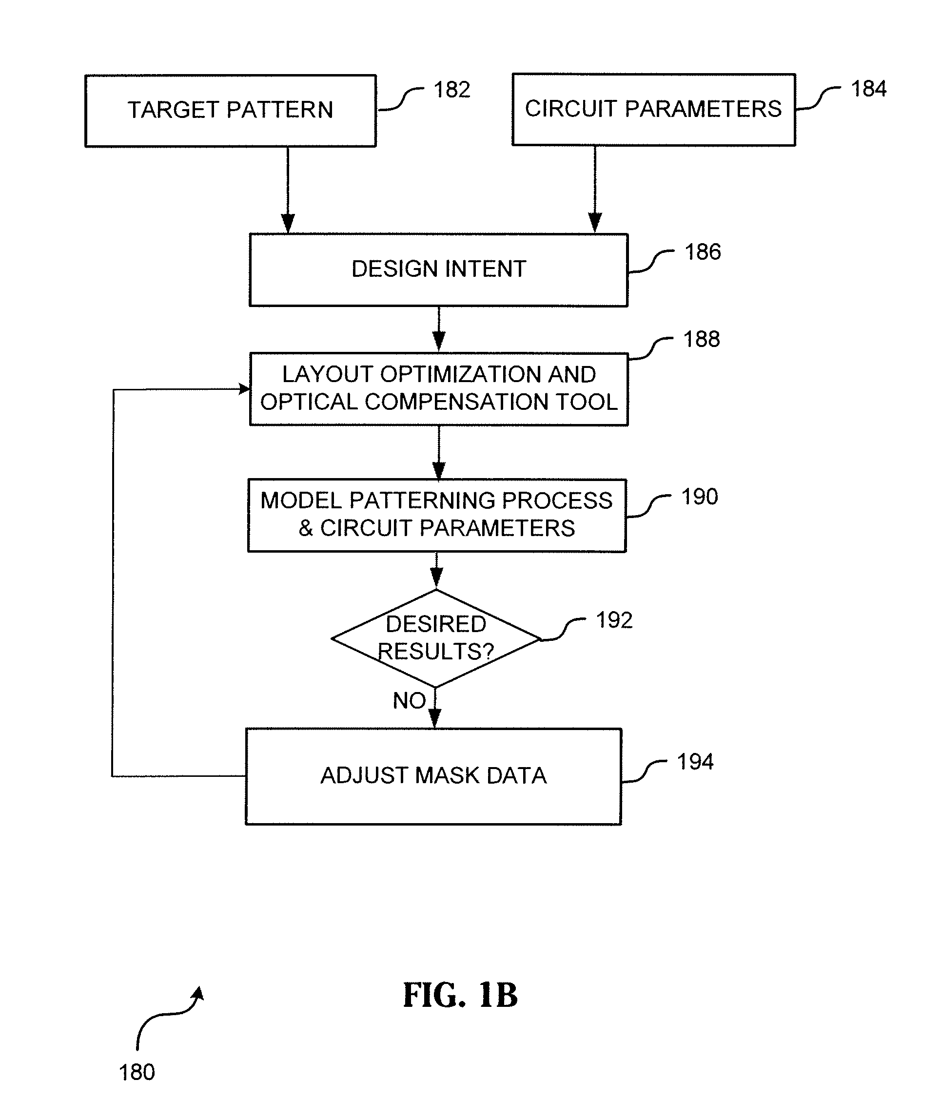
[0006]According to various embodiments of the invention, systems and methods for compensating proximity effect are provided. The method includes: providing a target pattern and target value for an electrical parameter of the circuit; simulating a lithographic patterning process and predicting a pattern that will be printed; calculating the electrical parameter for the predicted pattern; calculating a score that indicates how well the calculated electrical parameter matches its target value; and adjusting a data set that is used to manufacture a photomask in a way that improves the score.
[0007]In one embodiment, the method further performs: representing the photomask data as a set of polygons; segmenting an edge of a polygon; altering the polygon by moving a segment of its edge based on the calculated electrical parameter. In one embodiment, the electrical parameter comprises one or more parameters from the group consisting of saturation current, leakage current, threshold voltage, g...
PUM
 Abstract
Description
Claims
Application Information