Pixel and organic light emitting display device using the same

Active Publication Date: 2009-12-17
SAMSUNG DISPLAY CO LTD
View PDF5 Cites 27 Cited by
  • Summary
  • Abstract
  • Description
  • Claims
  • Application Information

AI Technical Summary

Benefits of technology

[0018]Another aspect of an embodiment according to the present invention provides an organic light emitting display device including: a scan driver for applying scan signals to a plurality of scan lines and for applying light emission control signals to a plurality of light emission control lines; a data driver for supplying a reset power voltage and for applying data signals to a plurality of data lines; and a plurality of pixels arranged at crossing regions of the plurality of data lines and the plurality of scan lines, wherein each of the plurality of pixels includes: an organic light emitting diode; a second transistor coupled between a first power source and the organic light emitting diode, the second transistor for controlling an amount of current supplied from the first power source to the organic light emitting diode; a third transistor coupled between a first electrode of the second transistor and the first power source, the third transistor configured to turn off when a light emission control signal is applied to a light emission control line coupled to a gate electrode of the third transistor; a first transistor coupled between a gate electrode of the second transistor and a data line, the first transistor configured to turn on when a scan signal is applied to a scan line coupled to a gate electrode of the first transistor; a first capacitor couple

Problems solved by technology

However, the pixel 4 of the conventional organic light emitting display device has difficulties displaying images with uniform luminance.
When the voltage from the first

Method used


Image

  • Pixel and organic light emitting display device using the same
  • Pixel and organic light emitting display device using the same
  • Pixel and organic light emitting display device using the same

Examples


Example

[0027]Hereinafter, certain exemplary embodiments according to the present invention will be described with reference to the accompanying drawings. Here, when a first element is described as being coupled to a second element, the first element may be directly coupled to the second element or may be indirectly coupled to the second element via one or more additional elements. Further, some of the elements that are not essential to the complete understanding of the invention are omitted for clarity. Also, like reference numerals refer to like elements throughout.

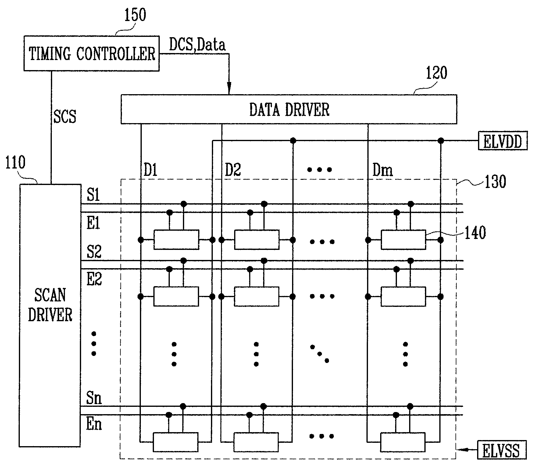
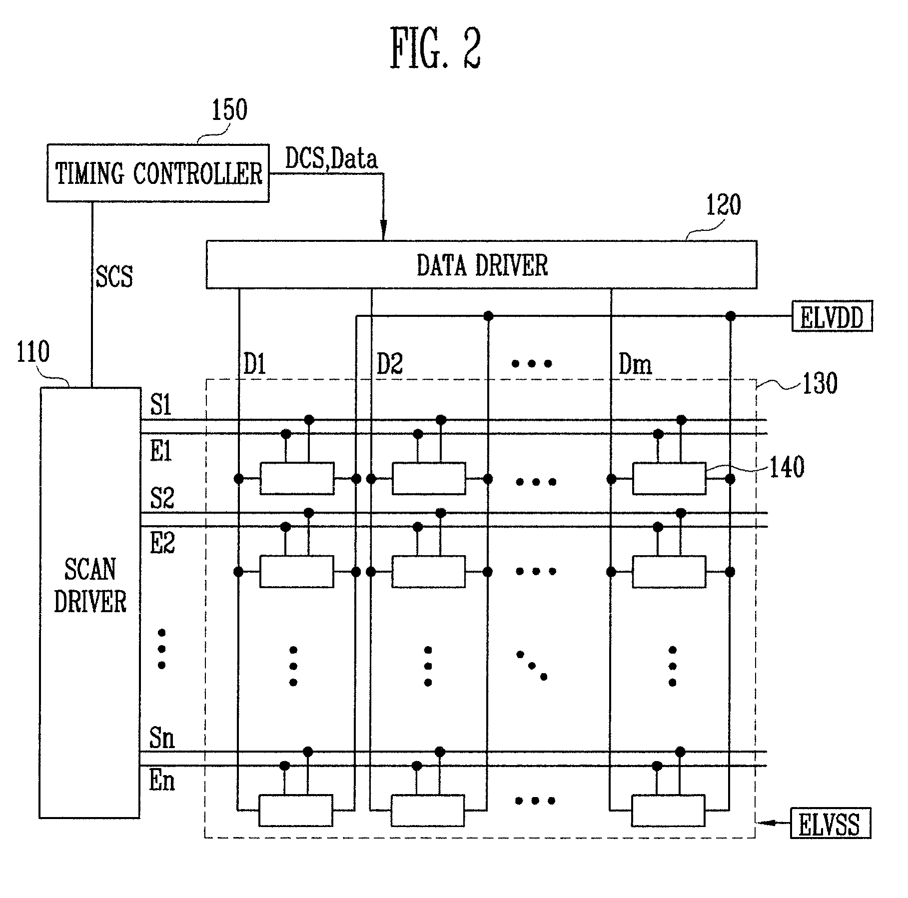
[0028]FIG. 2 is a schematic block diagram illustrating an organic light emitting display device according to one exemplary embodiment of the present invention.

[0029]Referring to FIG. 2, the organic light emitting display device according to one exemplary embodiment of the present invention includes a display unit 130 including pixels 140 arranged at crossing regions of scan lines (S1 to Sn) and data lines (D1 to Dm); a scan dri...


PUM


Abstract

A pixel for compensating for the threshold voltage of a drive transistor and the voltage drop of a first power source is provided. The pixel includes an organic light emitting diode; a driving transistor coupled between a first power source and the organic light emitting diode for controlling the current supplied to the organic light emitting diode; an emission control transistor coupled between a first electrode of the driving transistor and the first power source and configured to be turned off when a high light emission control signal is applied; a switching transistor coupled between a gate electrode of the driving transistor and a data line and configured to be turned on when a low scan signal is applied; a first capacitor coupled between the gate electrode of the driving transistor and the first electrode of the driving transistor; and a second capacitor coupled between the first electrode of the driving transistor and the first power source.

Description

CROSS-REFERENCE TO RELATED APPLICATION[0001]This application claims priority to and the benefit of Korean Patent Application No. 10-2008-0056812, filed on Jun. 17, 2008, in the Korean Intellectual Property Office, the entire content of which is incorporated herein by reference.BACKGROUND[0002]1. Field of the Invention[0003]The present invention relates to a pixel and an organic light emitting display device using the same.[0004]2. Discussion of Related Art[0005]In recent years, various flat panel display devices have been developed with reduced weight and volume as compared to cathode ray tubes. Types of flat panel display devices include liquid crystal display devices, field emission display devices, plasma display devices, and organic light emitting display devices, among others.[0006]Of these flat panel display devices, the organic light emitting display device displays an image by using organic light emitting diodes, which generate light by recombining electrons and holes. Organ...

Claims


Application Information

Patent Timeline
IPC IPC(8): G09G3/10H01J1/63
CPCG09G3/3233G09G2300/0819G09G2320/043G09G2300/0861G09G2300/0852H10B12/0335
Inventor KIM, YANG-WAN
Owner SAMSUNG DISPLAY CO LTD
Why Eureka
Try Eureka