
Multi-dimensional data registration integrated circuit for driving array-arrangement devices

an array array and data technology, applied in the direction of digital output to print units, instruments, computing, etc., can solve the problems of limiting the printing speed and allowable printhead number, two-dimensional driving circuits or one-dimensional driving circuits cannot meet such requirements, and the system of thermal-optical switches cannot meet the requirements for large amounts of data to be transmitted, stored, exchanged and processed at high speed. , to achieve the effect of reducing the number of external terminals

Inactive Publication Date: 2009-12-24
NATIONAL TSING HUA UNIVERSITY
View PDF2 Cites 20 Cited by
  • Summary
  • Abstract
  • Description
  • Claims
  • Application Information

AI Technical Summary

Benefits of technology

[0008]The present invention provides a multi-dimensional data registration integrated circuit for driving array-arrangement devices. It utilizes multi-dimensional or multi-hieratical circuit configuration to reduce the number of external terminals. Data is separately and sequentially output in a multiplex manner so that a large number of microelectronic devices arranged in an array can be controlled. Such an array is applicable to array-arrangement thermal-optical switches or a nozzle array device on an inkjet chip.
[0009]The present invention provides a multi-dimensional data registration integrated circuit capable of selecting processing signals. The data processing is performed in a manner whereby data is selected according to priority. The efficiency of the data registration of such a microelectronic device array is thereby improved.

Problems solved by technology

Unfortunately, the aforesaid two-dimensional driving circuit or one-dimensional driving circuit limits the printing speed and allowable printhead number.
However, it appears that the two-dimensional driving circuit or one-dimensional driving circuit cannot satisfy such requirements.
However, such a system of thermal-optical switches cannot satisfy the requirements for large amounts of data to be transmitted, stored, exchanged and processed at high speed.
Because the number of the thermal-optical switches is great, driving the resistors through direct current causes low reliability, low switch speed and temperature instability of the resistors.
Consequentially, the cost and failure rate of the package are increased.
However, if any of the external pads does not have a good electrical connection, the corresponding thermal-optical switches will fail to normally operate so that the designated paths of the waveguide cannot be heated.

Method used


Image

  • Multi-dimensional data registration integrated circuit for driving array-arrangement devices
  • Multi-dimensional data registration integrated circuit for driving array-arrangement devices
  • Multi-dimensional data registration integrated circuit for driving array-arrangement devices

Examples


Embodiment Construction

[0021]The following will demonstrate the present invention using the accompanying drawings to clearly present the characteristics of the technology.

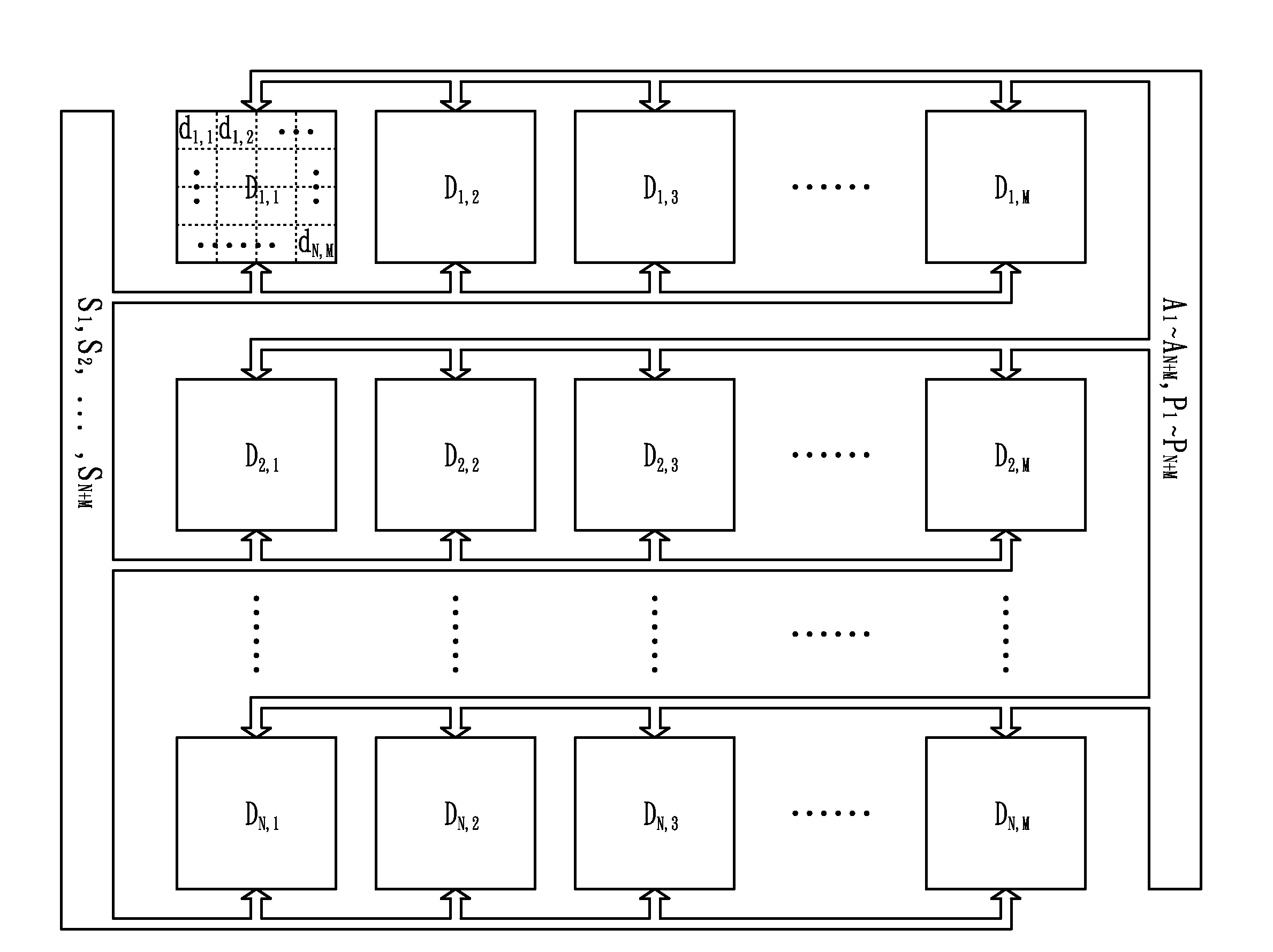
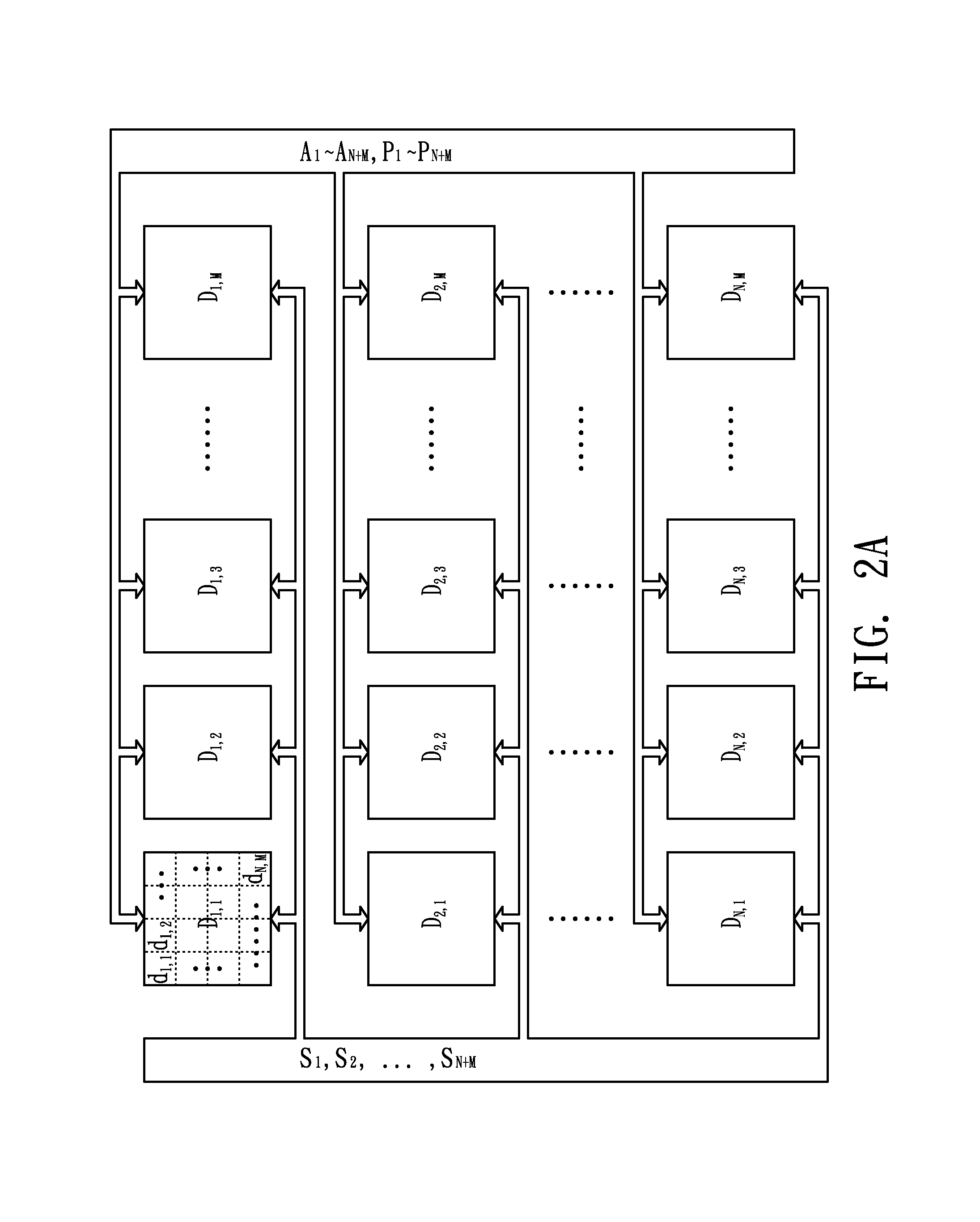
[0022]FIG. 2A is a schematic diagram of a multi-dimensional data registration integrated circuit for driving array-arrangement devices in accordance with the present invention. In this figure, D1,1, D1,2, . . . , DN,M represent a plurality of first hierarchy sets in which a plurality of array-arrangement devices are divided. Each of the first hierarchy sets comprises partial array-arrangement devices to be driven. Referring to numeral references 111 and 112 in FIG. 1, each device can be an assembly of switches such as a transistor and a resistor. In addition to the previous assembly, an alternative assembly comprises a resistor and a thermal-optical switch. S1, S1,2, . . . , SN,M represent first hierarchy address selection signals, which can scan and select the plurality of first hierarchy sets D1,1, D1,2, . . . , DN,M to be activated. A...


PUM


Abstract

A multi-dimensional data registration integrated circuit is configured for driving array-arrangement devices. The array-arrangement devices comprise a plurality of first hierarchy sets, each which comprises a plurality of second hierarchy sets. The multi-dimensional data registration integrated circuit comprises a first hierarchy address selection circuit, a second hierarchy address selection circuit and a data supply circuit. The first hierarchy address selection circuit scans the first hierarchy sets, and selects a unit of the first hierarchy sets to activate it. The second hierarchy address selection circuit scans the second hierarchy sets. The data supply circuit writes a plurality of data into each designated unit of the second hierarchy sets according to the scanning sequence of the second hierarchy address selection circuit.

Description

BACKGROUND OF THE INVENTION[0001](A) Field of the Invention[0002]The present invention relates to a multi-dimensional data registration integrated circuit for driving array-arrangement devices, and more particularly, to a multi-dimensional integration and multi-task chip for driving a large microelectronic array system.[0003](B) Description of the Related Art[0004]FIG. 1 is a schematic diagram of a traditional two-dimensional address selection circuit for driving 25 nozzles of a printhead. A two-dimensional address selection circuit 10 comprises a plurality of address selection lines A1-A5 and a plurality of data lines D1-D5. A plurality of array-arrangement control units 11 are at the intersections of the plurality of address selection lines A1-A5 and the plurality of data lines D1-D5. Each of the control units 11 comprises a transistor 111 and a resistor 112 for controlling a corresponding nozzle (not shown) to shoot a micro-scale ink droplet. When a transistor 111 is turned on by...

Claims


Application Information

Patent Timeline
IPC IPC(8): G06F3/12
CPCB41J2/04586B41J2/04541
Inventor TSENG, FAN GANGLIOU, JIAN CHIUN
Owner NATIONAL TSING HUA UNIVERSITY
Learn More